


AMD Geode™ SC1200/SC1201 Processor Data Book 71
4
General Configuration Block 32579B
4.0General Configuration Block
The General Configuration block includes registers for:
• Pin Multiplexing and Miscellaneous Configuration
• WATCHDOG Timer
• High-Resolution Timer
• Clock Generators
A selectable interrupt is shared by all these functions.
4.1 Configuration Block Addresses
Registers of the General Configuration block are I/O
mapped in a 64-byte address range. These registers are
physically connected to the internal Fast-PCI bus, but do
not have a register block in PCI configuration space (i.e.,
they do not appear to software as PCI registers).
After system reset, the Base Address register is located at
I/O address 02EAh. This address can be used only once.
Before accessing any PCI registers, the BOOT code must
program this 16-bit register to the I/O base address for the
General Configuration block registers. All subsequent
writes to this address, are ignored until system reset.
Note: Location of the General Configuration Block cannot
be determined by software. See the AMD Geode™
SC1200/SC1201 Processor Specification Update
document.
Reserved bits in the General Configuration block should be
read as written unless otherwise specified.
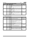
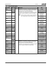
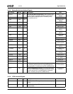
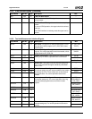
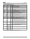
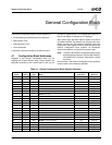
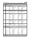
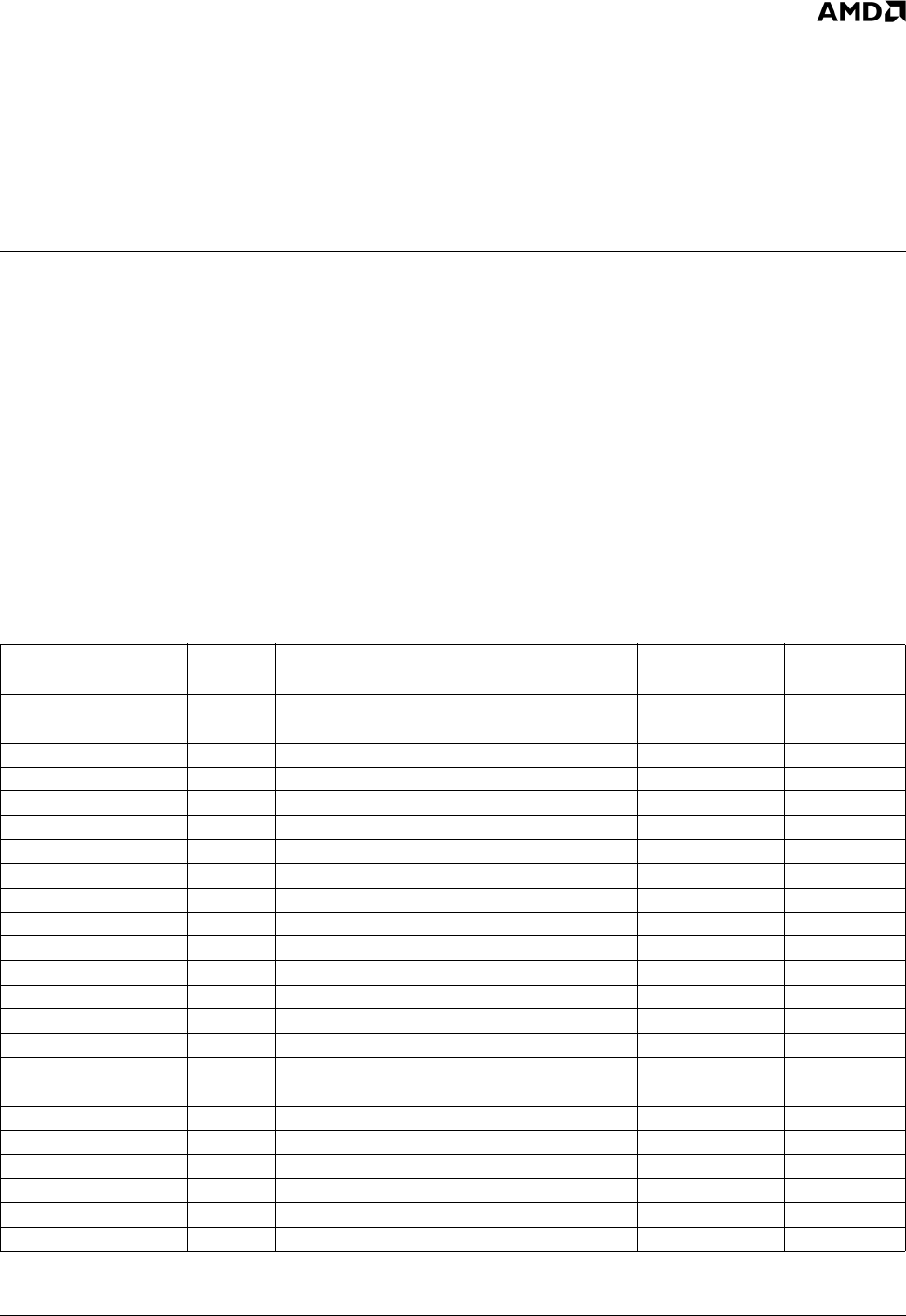
Table 4-1. General Configuration Block Register Summary
Offset
Width
(Bits) Type Name Reset Value Reference
00h-01h 16 R/W WDTO. WATCHDOG Timeout 0000h Page 80
02h-03h 16 R/W WDCNFG. WATCHDOG Configuration 0000h Page 80
04h 8 R/WC WDSTS. WATCHDOG Status 00h Page 81
05h-07h --- --- RSVD. Reserved --- ---
08h-0Bh 32 RO TMVALUE. TIMER Value xxxxxxxxh Page 82
0Ch 8 R/W TMSTS. TIMER Status 00h Page 82
0Dh 8 R/W TMCNFG. TIMER Configuration 00h Page 82
0Eh-0Fh --- --- RSVD. Reserved --- ---
10h 8 RO MCCM. Maximum Core Clock Multiplier Strapped Value Page 87
11h --- --- RSVD. Reserved --- ---
12h 8 R/W PPCR. PLL Power Control 2Fh Page 87
13h-17h --- --- RSVD. Reserved --- ---
18h-1Bh 32 R/W PLL3C. PLL3 Configuration E1040005h Page 87
1Ch-1Dh --- --- RSVD. Reserved --- ---
1Eh-1Fh 16 R/W CCFC. Core Clock Frequency Control Strapped Value Page 88
20h-2Fh --- --- RSVD. Reserved --- ---
30h-33h 32 R/W PMR. Pin Multiplexing Register 00000000h Page 72
34h-37h 32 R/W MCR. Miscellaneous Configuration Register 00000001h Page 76
38h 8 R/W INTSEL. Interrupt Selection 00h Page 78
39h-3Bh --- --- RSVD. Reserved --- ---
3Ch 8 RO ID. Device ID xxh Page 78
3Dh 8 RO REV. Revision xxh Page 78
3Eh-3Fh 16 RO CBA. Configuration Base Address xxxxh Page 78