154 AMD Geode™ SC1200/SC1201 Processor Data Book
Core Logic Module
32579B
DMA Addressing Capability
DMA transfers occur over the entire 32-bit address range of
the PCI bus. This is accomplished by using the DMA con-
troller’s 16-bit memory address registers in conjunction
with an 8-bit DMA Low Page register and an 8-bit DMA
High Page register. These registers, associated with each
channel, provide the 32-bit memory address capability. A
write to the Low Page register clears the High Page regis-
ter, for backward compatibility with the PC/AT standard.
The starting address for the DMA transfer must be pro-
grammed into the DMA controller registers and the chan-
nel’s respective Low and High Page registers prior to
beginning the DMA transfer.
DMA Page Registers and Extended Addressing
The DMA Page registers provide the upper address bits
during DMA cycles. DMA addresses do not increment or
decrement across page boundaries. Page boundaries for
the 8-bit channels (Channels 0 through 3) are every 64 KB
and page boundaries for the 16-bit channels (Channels 5,
6, and 7) are every 128 KB.
Before any DMA operations are performed, the Page regis-
ters must be written at the I/O Port addresses in the DMA
controller registers to select the correct page for each DMA
channel. The other address locations between 080h and
08Fh and 480h and 48Fh are not used by the DMA chan-
nels, but can be read or written by a PCI bus master. These
registers are reset to zero at POR. A write to the Low Page
register clears the High Page register, for backward com-
patibility with the PC/AT standard.
For most DMA transfers, the High Page register is set to
zeros and is driven onto PCI address bits AD[31:24] during
DMA cycles. This mode is backward compatible with the
PC/AT standard. For DMA extended transfers, the High
Page register is programmed and the values are driven
onto the PCI addresses AD[31:24] during DMA cycles to
allow access to the full 4 GB PCI address space.
DMA Address Generation
The DMA addresses are formed such that there is an
upper address, a middle address, and a lower address por-
tion.
The upper address portion, which selects a specific page,
is generated by the Page registers. The Page registers for
each channel must be set up by the system before a DMA
operation. The DMA Page register values are driven on
PCI address bits AD[31:16] for 8-bit channels and
AD[31:17] for 16-bit channels.
The middle address portion, which selects a block within
the page, is generated by the DMA controller at the begin-
ning of a DMA operation and any time the DMA address
increments or decrements through a block boundary. Block
sizes are 256 bytes for 8-bit channels (Channels 0 through
3) and 512 bytes for 16-bit channels (Channels 5, 6, and
7). The middle address bits are is driven on PCI address
bits AD[15:8] for 8-bit channels and AD[16:9] for 16-bit
channels.
The lower address portion is generated directly by the DMA
controller during DMA operations. The lower address bits
are output on PCI address bits AD[7:0] for 8-bit channels
and AD[8:1] for 16-bit channels.
BHE# is configured as an output during all DMA opera-
tions. It is driven as the inversion of AD0 during 8-bit DMA
cycles and forced low for all 16-bit DMA cycles.
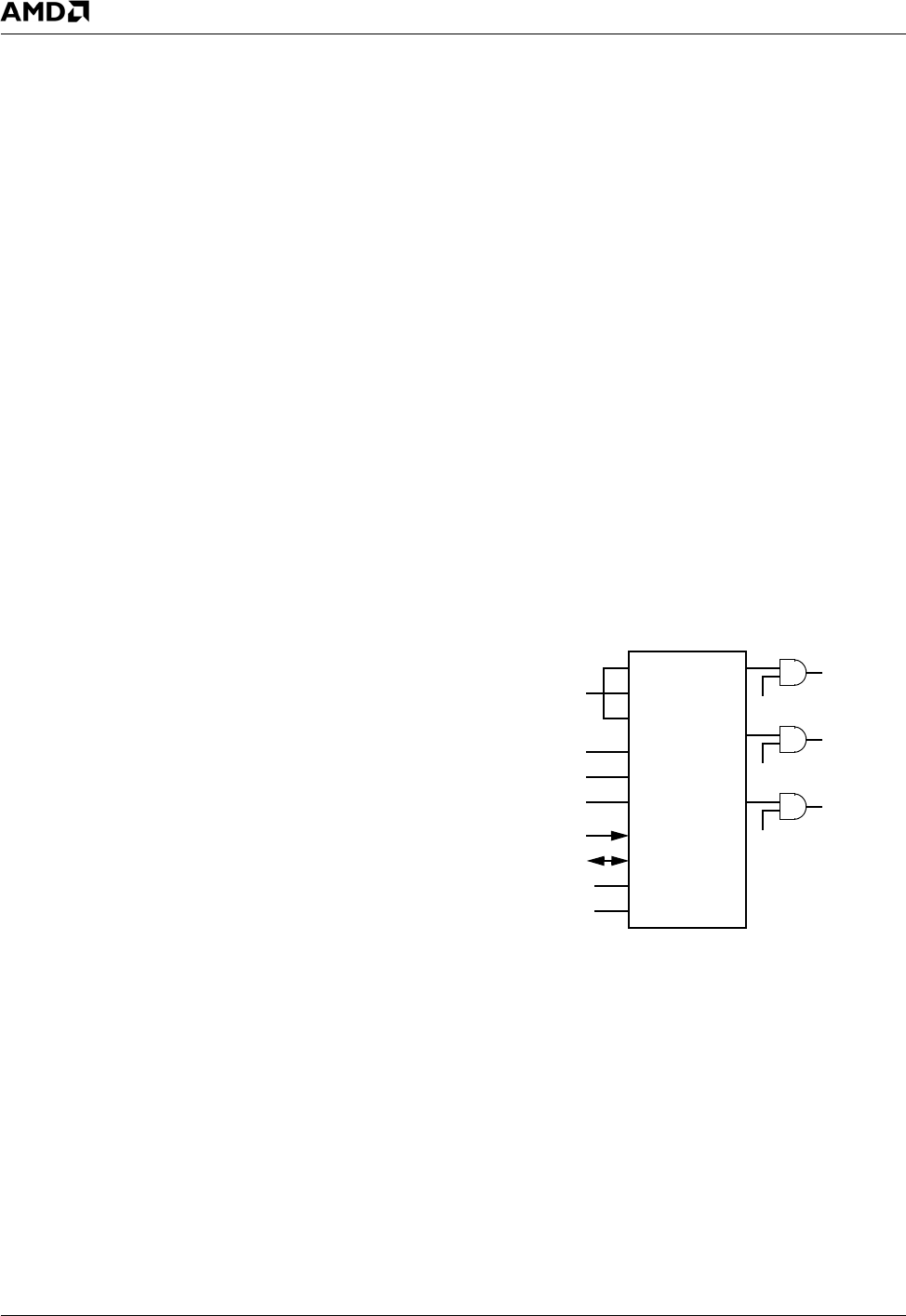
6.2.6.2 Programmable Interval Timer
The Core Logic module contains an 8254-equivalent Pro-
grammable Interval Timer (PIT) configured as shown in
Figure 6-7. The PIT has three timers/counters, each with
an input frequency of 1.19318 MHz (OSC divided by 12),
and individually programmable to different modes.
The gates of Counter 0 and 1 are usually enabled, how-
ever, they can be controlled via F0 Index 50h. The gate of
Counter 2 is connected to I/O Port 061h[0]. The output of
Counter 0 is connected internally to IRQ0. This timer is typ-
ically configured in Mode 3 (square wave output), and used
to generate IRQ0 at a periodic rate to be used as a system
timer function. The output of Counter 1 is connected to I/O
Port 061h[4]. The reset state of I/O Port 061h[4] is 0 and
every falling edge of Counter 1 output causes I/O Port
061h[4] to flip states. The output of Counter 2 is brought
out to the PC_BEEP output. This output is gated with I/O
Port 061h[1].
Figure 6-7. PIT Timer
PIT Shadow Register
The PIT registers are shadowed to allow for 0V Suspend to
save/restore the PIT state by reading the PIT’s counter and
write only registers. The read sequence for the shadow
register is listed in F0 Index BAh (see Table 6-29 on page
190).
CLK0
CLK1
CLK2
GATE0
GATE1
GATE2
XD[7:0]
A[1:0]
IOW#
IOR#
I/O Port 061h[1]
I/O Port 061h[0]
IRQ0
I/O Port
PC_BEEP
1.19318 MHz
WR#
RD#
OUT0
OUT1
OUT2
F0 Index 50h[4]
F0 Index 50h[6]
F0 Index 50h[3]
F0 Index 50h[5]
061h[4]


