AMD Geode™ SC1200/SC1201 Processor Data Book 175
Core Logic Module - PCI Configuration Space and Access
32579B
6.3 Register Descriptions
The Core Logic module is a multi-function module. Its reg-
ister space can be broadly divided into three categories in
which specific types of registers are located:
1) Chipset Register Space (F0-F5) (Note that F4 is for
Video Processor support, see Section 7.3.1 on page
333 for register descriptions): Comprised of six sepa-
rate functions, each with its own register space, con-
sisting of PCI header registers and configuration
registers.
The PCI header is a 256-byte region used for configur-
ing a PCI device or function. The first 64 bytes are the
same for all PCI devices and are predefined by the
PCI specification. These registers are used to config-
ure the PCI for the device. The rest of the 256-byte
region is used to configure the device or function itself.
2) USB Controller Register Space (PCIUSB): Consists of
the standard PCI header registers. The USB controller
supports three ports and is OpenHCI compliant.
3) ISA Legacy Register Space (I/O Ports): Contains all
the legacy compatibility I/O ports that are internal,
trapped, shadowed, or snooped.
The following subsections provide:
• A brief discussion on how to access the registers
located in PCI Configuration Space.
• Core Logic module register summaries.
• Bit formats for Core Logic module registers.
6.3.1 PCI Configuration Space and Access
Methods
Configuration cycles are generated in the processor. All
configuration registers in the Core Logic module are
accessed through the PCI interface using the PCI Type
One Configuration Mechanism. This mechanism uses two
DWORD I/O locations at 0CF8h and 0CFCh. The first loca-
tion (0CF8h) references the Configuration Address register.
The second location (0CFCh) references the Configuration
Data Register (CDR).
To access PCI configuration space, write the Configuration
Address (0CF8h) Register with data that specifies the Core
Logic module as the device on PCI being accessed, along
with the configuration register offset. On the following
cycle, a read or write to the Configuration Data Register
(CDR) causes a PCI configuration cycle to the Core Logic
module. Byte, WORD, or DWORD accesses are allowed to
CDR at 0CFCh, 0CFDh, 0CFEh, or 0CFFh.
The Core Logic module has seven PCI configuration regis-
ter sets, one for each function (F0-F5) and USB (PCIUSB).
Base Address Registers (BARx) in F0-F5 and PCIUSB set
the base addresses for additional I/O or memory mapped
configuration registers for each function.
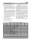
Table 6-13 shows the PCI Configuration Address Register
(0CF8h) and how to access the PCI header registers.
Table 6-13. PCI Configuration Address Register (0CF8h)
31 30 24 23 16 15 11 10 8 7 2 1 0
Configuration
Space Mapping Reserved Bus Number Device Number Function Index
DWORD
00
1 (Enable) 000 000 0000 0000 xxxx x (Note) xxx xxxx xx 00 (Always)
Function 0 (F0): Bridge Configuration, GPIO and LPC Configuration Register Space
80h 0000 0000 1001 0 or 1000 0 000 Index
Function 1 (F1): SMI Status and ACPI Timer Configuration Register Space
80h 0000 0000 1001 0 or 1000 0 001 Index
Function 2 (F2): IDE Controller Configuration Register Space
80h 0000 0000 1001 0 or 1000 0 010 Index
Function 3 (F3): Audio Configuration Register Space
80h 0000 0000 1001 0 or 1000 0 011 Index
Function 4 (F4): Video Processor Configuration Register Space
80h 0000 0000 1001 0 or 1000 0 100 Index
Function 5 (F5): X-Bus Expansion Configuration Register Space
80h 0000 0000 1001 0 or 1000 0 101 Index
PCIUSB: USB Controller Configuration Register Space
80h 0000 0000 1001 1 or 1000 1 000 Index
Note: The device number depends upon the IDSEL Strap Override bit (F5BAR0+I/O Offset 04h[0]). This bit allows selection of the
address lines to be used as the IDSEL. By Default: IDSEL = AD28 (1001 0) for F0-F5, AD29 (1001 1) for PCIUSB.


