346 AMD Geode™ SC1200/SC1201 Processor Data Book
Video Processor Module - Video Processor Registers - Function 4
32579B
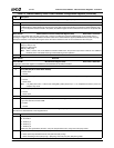
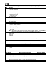
Offset 50h-53h Cursor Color Key Register (R/W) Reset Value: 00000000h
31:29 Reserved.
28:24 COLOR_REG_OFFSET (Cursor Color Register Offset). This field indicates a bit in the incoming graphics stream. It is
used to indicate which of the two possible cursor color registers should be used for color key matches for the bits in the
graphics stream.
23:0 CUR_COLOR_KEY (Cursor Color Key). Specifies the 24-bit RGB value of the cursor color key. The incoming graphics
stream is compared with this value. If a match is detected, the pixel is replaced by a 24-bit value from one of the Cursor
Color registers.
Offset 54h-57h Cursor Color Mask Register (R/W) Reset Value: 00000000h
31:24 Reserved.
23:0 CUR_COLOR_MASK (Cursor Color Mask). This mask is a 24-bit value. Zeroes in the mask cause the corresponding bits
in the incoming graphics stream to be ignored.
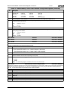
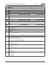
Offset 58h-5Bh Cursor Color Register 1 (R/W) Reset Value: 00000000h
31:24 Reserved.
23:0 CUR_COLOR_REG1 (Cursor Color Register 1). Specifies a 24-bit cursor color value. This is an RGB value (for RGB
blending) or a YUV value (for YUV blending). In interlaced YUV blending mode, Y/2 value should be used.
This is one of two possible cursor color values. The COLOR_REG_OFFSET bits (F4BAR0+Memory Offset 50h[28:24])
determine a bit of the graphics data that if even, selects this color to be used.
Offset 5Ch-5Fh Cursor Color Register 2 (R/W) Reset Value: 00000000h
31:24 Reserved.
23:0 CUR_COLOR_REG2 (Cursor Color Register 2). Specifies a 24-bit cursor color value. This is an RGB value (for RGB
blending) or a YUV value (for YUV blending). In interlaced YUV blending mode, Y/2 value should be used.
This is one of two possible cursor color values. The COLOR_REG_OFFSET bits (F4BAR0+Memory Offset 50h[28:24])
determine a bit of the graphics data that if even, selects this color to be used.
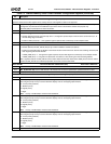
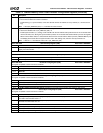
Offset 60h-63h Alpha Window 1 X Position Register (R/W) Reset Value: 00000000h
Note: H_TOTAL and H_SYNC_END are values programmed in the GX1 module’s Display Controller Timing registers
(GX_BASE+Memory Offset 8330h[26:19] and 8338h[10:3], respectively). The value of (H_TOTAL – H_SYNC_END) is some-
times referred to as “horizontal back porch”. For more information, see the AMD Geode™ GX1 Processor Data Book.
Desired screen position should not be outside a video window (F4BAR0+Memory Offset 08h and 0Ch).
31:27 Reserved.
26:16 ALPHA1_X_END (Alpha Window 1 Horizontal End). Determines the horizontal end position of Alpha Window 1 (not inclu-
sive). This value is calculated according to the following formula:
Value = Desired screen position + (H_TOTAL – H_SYNC_END) – 1.
15:11 Reserved.
10:0 ALPHA1_X_START (Alpha Window 1 Horizontal Start). Determines the horizontal start position of Alpha Window 1. This
value is calculated according to the following formula:
Value = Desired screen position + (H_TOTAL – H_SYNC_END) – 2.
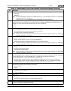
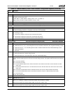
Offset 64h-67h Alpha Window 1 Y Position Register (R/W) Reset Value: 00000000h
Note: V_TOTAL and V_SYNC_END are values programmed in the GX1 module’s Display Controller Timing registers
(GX_BASE+Memory Offset 8340h[26:16] and 8348h[26:16], respectively). The value of (V_TOTAL – V_SYNC_END) is some-
times referred to as “vertical back porch”. For more information, see the AMD Geode™ GX1 Processor Data Book.
Desired screen position should not be outside a video window (F4BAR0+Memory Offset 08h and 0Ch).
31:27
Reserved.
26:16 ALPHA1_Y_END (Alpha Window 1 Vertical End). Determines the vertical end position of Alpha Window 1 (not inclusive).
This value is calculated according to the following formula:
Value = Desired screen position + (V_TOTAL – V_SYNC_END) + 2.
15:11 Reserved.
10:0 ALPHA1_Y_START (Alpha Window 1 Vertical Start). Determines the vertical start position of Alpha Window 1. This value
is calculated according to the following formula:
Value = Desired screen position + (V_TOTAL – V_SYNC_END) + 1.
Table 7-9. F4BAR0+Memory Offset: Video Processor Configuration Registers (Continued)
Bit Description


