


AMD Geode™ SC1200/SC1201 Processor Data Book 25
3
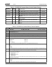
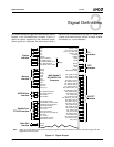
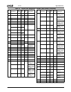
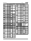
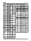
Signal Definitions 32579B
3.0Signal Definitions
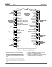
This section defines the signals and describes the external
interface of the SC1200/SC1201 processor. Figure 2-1
shows the signals organized by their functional groups.
Where signals are multiplexed, the default signal name is
listed first and is separated by a plus sign (+). A slash (/) in
a signal name means that the function is always enabled
and available (i.e., cycle multiplexed).
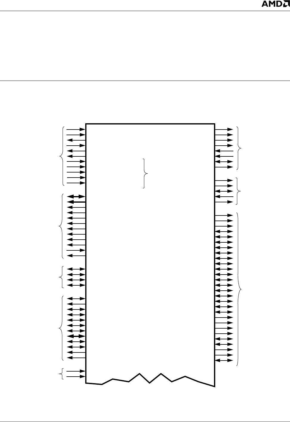
Figure 3-1. Signal Groups
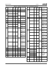
System
POR#
X32I
X27I
MD[63:0]
MA[12:0]
BA[1:0]
CS[1:0]#
RASA#
CASA#
WEA#
DQM[7:0]
CKEA
SDCLK[3:0]
SDCLK_IN
SDCLK_OUT
ACCESS.bus
AB1C+GPIO20+DOCCS#
AB1D+GPIO1+IOCS1#
GPIO12+AB2C
GPIO13+AB2D
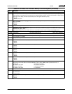
CRT
HSYNC
VSYNC
VREF
SETRES
RED, GREEN, BLUE
PCIRST#
ACK#+TFTDE+VOPCK
AFD#/DSTRB#+TFTD2+VOPD1
BUSY/WAIT#+TFTD3+VOPD2
ERR#+TFTD4+VOPD3
INIT#+TFTD5+VOPD4
PD[5:0]+TFTD[11:6]+VOPD[7:5]
PE+TFTD14
SLCT+TFTD15
SLIN#/ASTRB#+TFTD16
STB#/WRITE#+TFTD17
Parallel Port/
IDE_ADDR2+TFTD4
IDE_DATA15+TFTD7
IDE_IOR0#+TFTD10
IDE_IOW0#+TFTD9
IDE_CS0#+TFTD5
IDE_IORDY0+TFTD11
IDE_DREQ0+TFTD8
IDE_DACK0#+TFTD0
IRQ14+TFTD1
IDE/TFT
IDE_CS1#+TFTDE
IDE_DATA12+TFTD13
IDE_DATA10+DDC_SCL
IDE_DATA14+TFTD17
IDE_DATA13+TFTD15
IDE_DATA11+GPIO41
IDE_DATA9+DDC_SDA
IDE_DATA8+GPIO40
IDE_DATA7+INTD#
IDE_DATA6+IRQ9
IDE_DATA5+CLK27M
IDE_DATA4+FP_VDD_ON
IDE_DATA3+TFTD12
IDE_DATA2+TFTD14
IDE_DATA1+TFTD16
IDE_DATA0+TFTD6
IDE_ADDR1+TFTD2
IDE_ADDR0+TFTD3
IDE_RST#+TFTDCK
PD6+TFTD1+VOPD0
PD7+TFTD13
X32O
X27O
TV
CVBS+Cr+TVB
SVY+Cb+TVR+CVBS
SVC+Cr+Cb+TVB+TVR
CVBS+Y+TVG
TVCOMP
TVRSET
TVREF
TVIOM
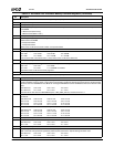
Memory
Interface
Interface
Interface
TFT/VOP Interface
Interface
Interface
Interface
VPD[7:0]
VPCKIN
Video Port
Interface
AMD Geode™
SC1200/SC1201
Processor
BOOT16+ROMCS#
LPC_ROM+PCICLK1
TFT_PRSNT+SDATA_OUT
FPCI_MON+PCICLK0
DID0+GNT0#, DID1+GNT1#
Straps
Note: Straps are not the default signal, shown with system signals for reader convenience. However, also listed in figure with the
appropriate functional group.