AMD Geode™ SC1200/SC1201 Processor Data Book 281
Core Logic Module - X-Bus Expansion Interface - Function 5
32579B
6.4.5.1 X-Bus Expansion Support Registers
F5 Index 10h, Base Address Register 0 (F5BAR0) set the
base address that allows PCI access to additional I/O Con-
trol support registers. Table 6-40 shows the support regis-
ters accessed through F5BAR0.
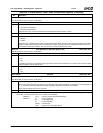
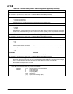
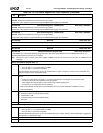
Table 6-40. F5BAR0+I/O Offset: X-Bus Expansion Registers
Bit Description
Offset 00h-03h I/O Control Register 1 (R/W) Reset Value: 010C0007h
31:28 Reserved.
27 IO_ENABLE_SIO_IR (Enable Integrated SIO Infrared).
0: Disable.
1: Enable.
26:25 IO_SIOCFG_IN (Integrated SIO Input Configuration). These two bits can be used to disable the integrated SIO totally or
limit/control the base address.
00: Integrated SIO disable.
01: Integrated SIO configuration access disable.
10: Integrated SIO base address 02Eh/02Fh enable.
11: Integrated SIO base address 015Ch/015Dh enable.
24 IO_ENABLE_SIO_DRIVING_ISA_BUS (Enable Integrated SIO ISA Bus Control). Allow the integrated SIO to drive the
internal ISA bus.
0: Disable.
1: Enable. (Default)
23:21 Reserved. Set to 0.
20 IO_USB_SMI_PWM_EN (USB Internal SMI). Route USB-generated SMI to SMI Status Register in F1BAR0+I/O Offset
00h/02h[14].
0: Disable.
1: Enable.
19 IO_USB_SMI_EN (USB SMI Configuration). Allow USB-generated SMIs.
0: Disable
1: Enable.
If bits 19 and 20 are enabled, the SMI generated by the USB is reported via the Top Level SMI status register at F1BAR0+I/
O Offset 00h/02h[14].
If only bit 19 is enabled, the USB can generate an SMI but there is no status reporting.
18 IO_USB_PCI_EN (USB). Enables USB ports.
0: Disable.
1: Enable.
17:0 Reserved.
Offset 04h-07h I/O Control Register 2 (R/W) Reset Value: 00000002h
31:2 Reserved. Write as read.
1 Video Processor Access Enable. Allows access to video processor using F4BAR0.
0: Disable.
1: Enable. (Default)
Note: This bit is readable after the register (F5BAR0+Offset 04h) has been written once.
0 IO_STRAP_IDSEL_SELECT (IDSEL Strap Override).
0: IDSEL: AD28 for Chipset Register Space (F0-F5), AD29 for USB Register Space (PCIUSB).
1: IDSEL: AD26 for Chipset Register Space (F0-F5), AD27 for USB Register Space (PCIUSB).


