


44 AMD Geode™ SC1200/SC1201 Processor Data Book
Signal Definitions
32579B
3.2 Strap Options
Several balls are read at power-up that set up the state of
the SC1200/SC1201 processor. These balls are typically
multiplexed with other functions that are outputs after the
power-up sequence is complete. The SC1200/SC1201 pro-
cessor must read the state of the balls at power-up and the
internal PU or PD resistors do not guarantee the correct
state will be read. Therefore, it is required that an external
PU or PD resistor with a value of 1.5 KΩ be placed on the
balls listed in Table 3-4. The value of the resistor is impor-
tant to ensure that the proper state is read during the
power-up sequence. If the ball is not read correctly at
power-up, the SC1200/SC1201 processor may default to a
state that causes it to function improperly, possibly result-
ing in application failure.
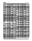
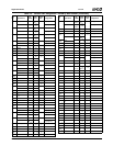
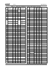
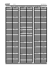
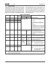
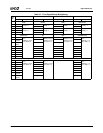
Table 3-4. Strap Options
Strap Option Muxed With Ball No.
Nominal
Internal
PU or PD
External PU/PD Strap Settings
Register ReferencesStrap = 0 (PD) Strap = 1 (PU)
CLKSEL0 RD# B8 PD
100
See Table 4-7 on page 85 for
CLKSEL strap options.
GCB+I/O Offset 1Eh[9:8] (aka CCFC register
bits [9:8]) (RO): Value programmed at reset
by
CLKSEL[1:0].
GCB+I/O Offset 10h[3:0] (aka MCCM regis-
ter bits [3:0]) (RO): Value programmed at
reset by
CLKSEL[3:0].
GCB+I/O Offset 1Eh[3:0] (aka CCFC register
bits [3:0]) (R/W, but write not recommended):
Value programmed at reset by CLKSEL[3:0].
Note: Values for GCB+I/O Offset 10h[3:0]
and 1Eh[3:0] are not the same.
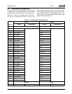
CLKSEL1 SOUT1 AF3 PD
100
CLKSEL2 SOUT2 D29 PD
100
CLKSEL3 SYNC P30 PD
100
BOOT16 ROMCS# C8 PD
100
Enable boot
from 8-bit ROM
Enable boot
from 16-bit
ROM
GCB+I/O Offset 34h[3] (aka MCR register bit
3) (RO): Reads back strap setting.
GCB+I/O Offset 34h[14] (R/W): Used to allow
the ROMCS# width to be changed under pro-
gram control.
TFT_PRSNT SDATA_OUT P29 PD
100
TFT not muxed
onto Parallel
Port
TFT muxed
onto Parallel
Port
GCB+I/O Offset 30h[23] (aka PMR register
bit 23) (R/W): Reads back strap setting.
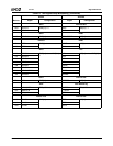
LPC_ROM PCICLK1 D6 PD
100
Disable boot
from ROM on
LPC bus
Enable boot
from ROM on
LPC bus
F0BAR1+I/O Offset 10h[15] (R/W): Reads
back strap setting and allows LPC ROM to be
changed under program control.
FPCI_MON PCICLK0 A4 PD
100
Disable Fast-
PCI, INTR_O,
and SMI_O
monitoring sig-
nals.
Enable Fast-
PCI, INTR_O,
and SMI_O
monitoring sig-
nals. (Useful
during debug.)
GCB+I/O Offset 34h[30] (aka MCR register
bit 30) (RO): Reads back strap setting.
Note: For normal operation, strap this sig-
nal low using a 1.5 KΩ resistor.
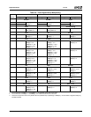
DID0 GNT0# C5 PD
100
Defines the system-level chip ID. GCB+I/O Offset 34h[31,29] (aka MCR regis-
ter bits 31 and 29) (RO): Reads back strap
setting.
Note: These signals should be connected
to a 1.5 KΩ PD resistor to ensure a
low level at power-up.
DID1 GNT1# C6 PD
100
Note: Accuracy of internal PU/PD resistors: 80K to 250K.
Location of the GCB (General Configuration Block) cannot be determined by software. See the AMD Geode™ SC1200/SC1201
Processor Specification Update document.