


Hardware Description
ARM DUI 0125A
© Copyright ARM Limited 1999. All rights reserved.
3-5
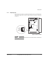
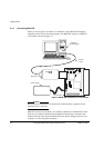
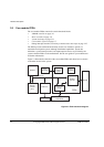
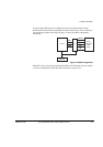
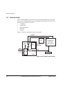
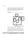
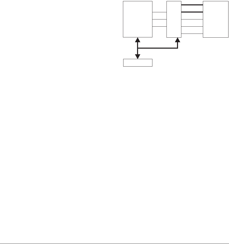
At power-up the FPGA loads its configuration data from a flash memory device.
Parallel data from the flash is serialized by the Programmable Logic Device (PLD) into
the configuration inputs of the FPGA. Figure 3-2 shows the FPGA configuration
mechanism.
Figure 3-2 FPGA configuration
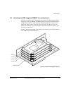
Multi-ICE can be used to reprogram the PLD, FPGA, and flash when the core module
is placed in configuration mode. See Multi-ICE support on page 3-21.
FPGA
FPGA
configuration
ROM
(flash)
PLD
Multi-ICE
DIN
CCLK
DONE
D[7:0]
A[18:0]
OE
WE
CS