


Programmer’s Reference
ARM DUI 0125A
© Copyright ARM Limited 1999. All rights reserved.
4-15
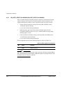
Note
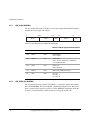
Before the SDRAM is used it is necessary to read the SPD memory and program the
CM_SDRAM register with the parameters indicated in Table 4-8. If these values are not
correctly set then SDRAM accesses may be slow or unreliable. See CM_SPD
(0x10000100 to 0x100001FC) on page 4-16.
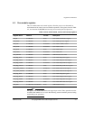
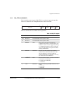
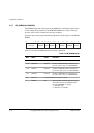
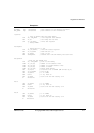
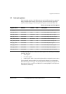
4:2
MEMSIZE
Read/write These bits specify the size of the SDRAM
module fitted to the core module. The bits are
encoded as follows:
000 = 16MB
001 = 32MB
010 = 64MB (default)
011 = 128MB
100 = 256MB
101 = Reserved
110 = Reserved.
1:0 CASLAT Read/write These bits specify the CAS latency set for the
core module. The bits are encoded as follows:
00 = Reserved
01 = Reserved
10 = 2 cycles (default)
11 = 3 cycles.
Table 4-8 CM_SDRAM register (continued)
Bits Name Access Function