


Hardware Description
3-12
© Copyright ARM Limited 1999. All rights reserved.
ARM DUI 0125A
Write transactions from the processor to the system bus normally complete on the local
memory bus in a single cycle. The data, address, and control information associated
with the transfer are posted into FIFO, and the transfer on the system bus occurs some
time later when that bus is available. This means that system bus error responses to
write transfers are not reported back to the processor as data aborts. If the FIFO is full,
the processor receives a wait response until space becomes available.
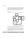
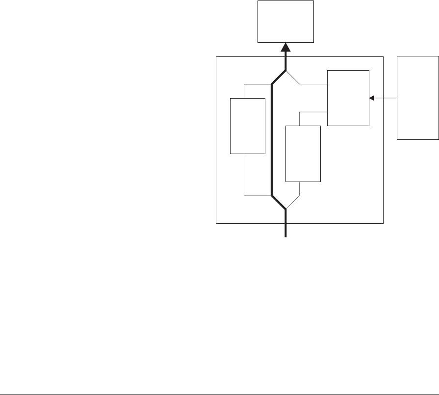
Processor reads
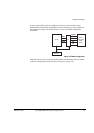
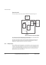
The data routing for processor reads from the system bus is illustrated in Figure 3-5.
Figure 3-5 Processor reads from the system bus
For reads from the system bus, the address and control information also pass through
the FIFO. The returned data from the system bus bypasses the FIFO.
The order of processor transactions is preserved on the system bus. Any previously
posted writes are drained from the FIFO (that is, completed on the system bus) before
the read transfer is performed. The processor receives a wait response until the read
transfer has completed on the system bus, when it receives the data and any associated
bus error response from the system bus. For information about SDRAM addresses, see
SDRAM accesses on page 4-4.
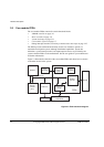
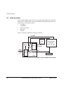
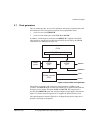
Processor
core
SDRAM
controller
Motherboard
SDRAM
FIFO
FIFO