System Control Coprocessor
ARM DDI 0363E Copyright © 2009 ARM Limited. All rights reserved. 4-16
ID013010 Non-Confidential, Unrestricted Access
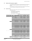
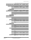
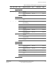
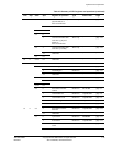
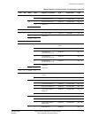
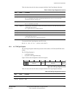
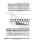
Table 4-4 shows how the bit values correspond with the Cache Type Register functions.
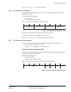
To access the Cache Type Register, read CP15 with:
MRC p15, 0, <Rd>, c0, c0, 1 ; Returns cache details
4.2.4 c0, TCM Type Register
The TCM Type Register informs the processor of the number of ATCMs and BTCMs in the
system.
The TCM Type Register is:
• a read-only register
• accessible in Privileged mode only.
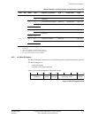
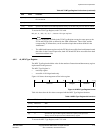
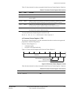
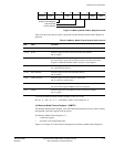
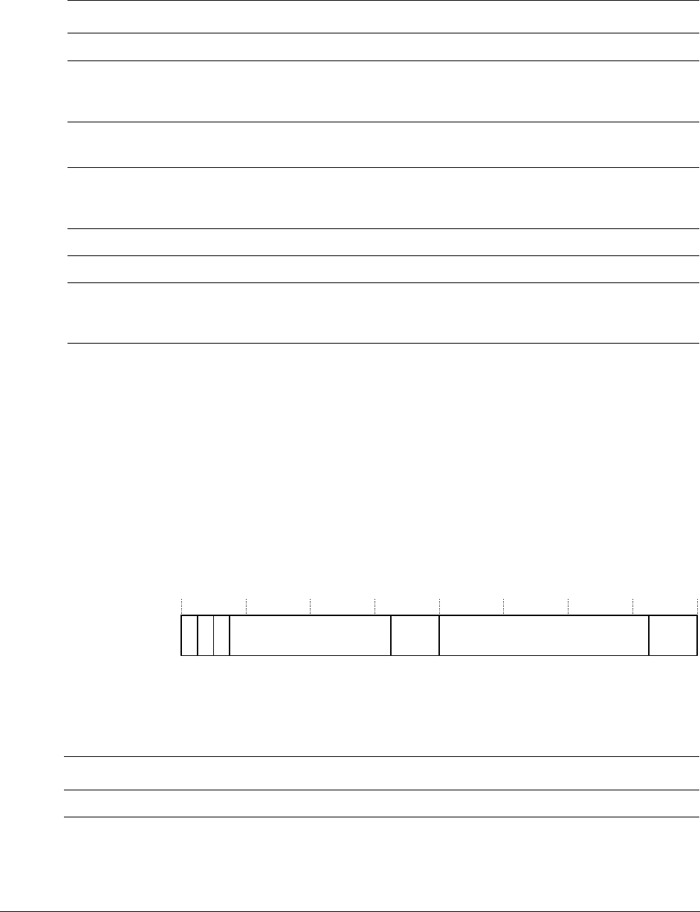
Figure 4-9 shows the arrangement of bits in the register.
Figure 4-9 TCM Type Register format
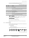
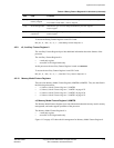
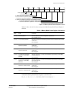
Table 4-5 shows how the bit values correspond with the TCM Type Register functions.
Table 4-4 Cache Type Register bit functions
Bits Field Function
[31:28] - Always b1000.
[27:24] CWG Cache Write-back Granule
0x0
= no information provided. See maximum cache line size in c0, Current Cache Size
Identification Register on page 4-32.
[23:20] ERG Exclusives Reservation Granule
0x0
= no information provided.
[19:16] DMinLine Indicates log2 of the number of words in the smallest cache line of the data and unified caches
controlled by the processor:
0x3
= eight words in an L1 data cache line.
[15:14] - Always
0x3
.
[13: 4] - Always
0x000
.
[3: 0] IMinLine Indicates log2 of the number of words in the smallest cache line of the instruction caches
controlled by the processor:
0x3
- eight words in an L1 instruction cache line.
0
31
30
29 28 19 18 16 15 3 2 0
0 0 Reserved BTCM Reserved ATCM
Table 4-5 TCM Type Register bit functions
Bits Field Function
[31:29] - Always 0.
[28:19] Reserved SBZ.


