


Level One Memory System
ARM DDI 0363E Copyright © 2009 ARM Limited. All rights reserved. 8-31
ID013010 Non-Confidential, Unrestricted Access
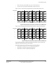
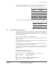
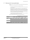
Table 8-15 shows the organization for the data cache when ECC is implemented. For ECC error
detection, seven bits are added per 32 bits, so seven bits are added for each RAM bank.
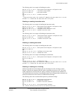
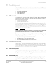
Table 8-16 shows the organization of the data cache RAM bits when ECC is implemented.
8.5.5 Cache interaction with memory system
This section describes how to enable or disable the cache RAMs, and to enable or disable error
checking. After you enable or disable the instruction cache, you must issue an
ISB
instruction to
flush the pipeline. This ensures that all subsequent instruction fetches see the effect of enabling
or disabling the instruction cache.
After reset, you must invalidate each cache before enabling it.
When disabling the data cache, you must clean the entire cache to ensure that any dirty data is
flushed to L2 memory.
Before enabling the data cache, you must invalidate the entire data cache if L2 memory might
have changed since the cache was disabled.
Before enabling the instruction cache, you must invalidate the entire instruction cache if L2
memory might have changed since the cache was disabled.
See Enabling or disabling AXI slave accesses on page 9-23 and Accessing RAMs using the AXI
slave interface on page 9-24 for information about how to access the cache RAMs using the
AXI slave interface.
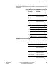
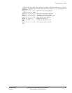
Disabling or enabling all of the caches
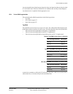
The following code is an example of enabling caches:
MRC p15, 0, R1, c1, c0, 0 ; Read System Control Register configuration data
ORR R1, R1, #0x1 <<12 ; instruction cache enable
ORR R1, R1, #0x1 <<2 ; data cache enable
DSB
MCR p15, 0, r0, c15, c5, 0 ; Invalidate entire data cache
MCR p15, 0, r0, c7, c5, 0 ; Invalidate entire instruction cache
MCR p15, 0, R1, c1, c0, 0 ; enabled cache RAMs
ISB
Table 8-15 Data cache data RAM sizes with ECC
Cache size Data RAMs
4KB, 4 1KB ways 8 banks 39 bits 128 lines
8KB, 4 2KB ways 8 banks 39 bits 256 lines
16KB, 4 4KB ways 8 banks 39 bits 512 lines
32KB, 4 8KB ways 8 banks 39 bits 1024 lines
64KB, 4 16KB ways 8 banks 39 bits 2048 lines
Table 8-16 Data cache RAM bits, with ECC
RAM bits Description
Bits [39:32] ECC code bits for data [31:0]
Bits [31:0] Data [31:0]