


Processor Signal Descriptions
ARM DDI 0363E Copyright © 2009 ARM Limited. All rights reserved. A-17
ID013010 Non-Confidential, Unrestricted Access
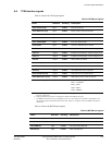
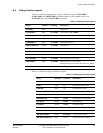
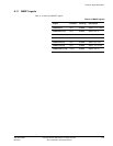
A.8 Debug interface signals
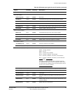
Table A-12 shows the debug interface signals. With the exception of PCLKDBG,
PCLKENDBG and PRESETDBGn, all these signals are only sampled or driven on
PCLKDBG edges when PCLKENDBG is asserted.
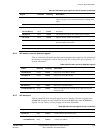
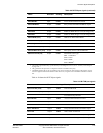
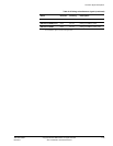
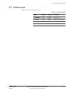
Table A-13 shows the debug miscellaneous signals.
Table A-12 Debug interface signals
Signal Direction Clocking Description
PCLKDBG Input - Debug clock.
PCLKENDBG Input PCLKDBG Clock enable for PCLKDBG.
PSELDBG Input PCLKDBG Selects the external debug interface.
PADDRDBG[11:2] Input PCLKDBG Programming address.
PADDRDBG31 Input PCLKDBG Programming address.
PRDATADBG[31:0] Output PCLKDBG
Read data bus.
PWDATADBG[31:0] Input PCLKDBG Write data bus.
PENABLEDBG Input PCLKDBG Indicates second, and subsequent, cycle of a transfer.
PREADYDBG Output PCLKDBG Extends a APB transfer by the inserting wait states.
PSLVERRDBG Output PCLKDBG Slave-generated error response.
PWRITEDBG Input PCLKDBG Indicates access is a write transfer.
Distinguishes between a read, LOW, and a write, HIGH.
PRESETDBGn Input Any Reset debug logic.
Table A-13 Debug miscellaneous signals
Name Direction Clocking Description
DBGEN Input Any Debug enable
NIDEN Input Any Non-invasive debug enable
EDBGRQ Input Any External debug request
DBGACK Output CLKIN Debug acknowledge
DBGRSTREQ
a
Output PCLKDBG Request for reset from debug logic
DBGTRIGGER Output CLKIN External debug request taken
COMMRX Output CLKIN Write-DTR full
COMMTX Output CLKIN Read-DTR empty
DBGRESTART Input External restart request
DBGRESTARTED Output CLKIN Handshake for DBGRESTART
DBGNOPWRDWN Output PCLKDBG No power-down request
DBGROMADDR[31:12] Input Tie-off Debug ROM physical address