


FPU Programmer’s Model
ARM DDI 0363E Copyright © 2009 ARM Limited. All rights reserved. 12-3
ID013010 Non-Confidential, Unrestricted Access
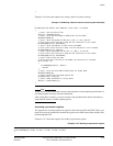
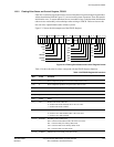
12.2 General-purpose registers
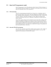
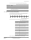
The FPU implements a VFP register bank. This bank is distinct from the ARM register bank.
You can reference the VFP register bank using two explicitly aliased views. Figure 12-1 shows
the two views of the register bank and the way the word and doubleword registers overlap.
12.2.1 FPU views of the register bank
In the FPU, you can view the register bank as:
• Sixteen 64-bit doubleword registers,
D0-D15
.
• Thirty-two 32-bit single-word registers,
S0-S31
.
• A combination of registers from the above views.
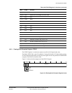
Figure 12-1 FPU register bank
The mapping between the registers is as follows:
•
S<2n>
maps to the least significant half of
D<n>
•
S<2n+1>
maps to the most significant half of
D<n>
.
For example, you can access the least significant half of the value in
D6
by accessing
S12
, and
the most significant half of the elements by accessing
S13
.
...
D0
D1
D2
D3
D14
D15
S0
S1
S2
S3
S4
S5
S6
S7
S28
S29
S30
S31
...