TELEPHONE INTERFACE MODULE (TIM)
14-8
14.4 E&M LEAD CIRCUIT THEORY OF
OPERATION
14.4.1 E&M INTERFACE
This card was designed to mate with any of the
five available E&M signaling formats. E&M
signaling usually requires a -48V supply with positive
ground and must have some type of current limiting
available. Q205 and Q204 are a bipolar constant
current source used for current limiting.
CR201, CR202 and CR203 are 68V, 0.5W zener
diodes that act with RV202-RV208 to provide electro-
static discharge protection. These devices ground any
voltage spikes caused from back-EMF associated with
driving relay type E&M systems.
The basic switching for this card comes from
Q202/Q203 (a complementary Darlington pair). With
S201 (8-position DIP switch) the relative configura-
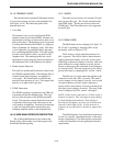
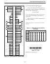
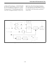
tion of Q202/Q203 can be manipulated. Figure 14-11
is an “equivalent switching” diagram for a TYPE III
configuration.
The drive for Q202 and Q203 is from optoisola-
tors U213/U214. Q206 is used only in Type V inter-
face where an inversion is required to drive Q202.
The E-Lead current sensor consists of current
limit resistor R219 and an optoisolator U212. CR205
is for reverse voltage protection for the optoisolator
and LED CR204.
Figure 14-11 TYPE III INTERFACE
14.4.2 SIGNAL CONDITIONING
Q201 inverts the logic to the Schmitt buffer
U211. The buffer output is used to charge and
discharge C227 through R230 and the series output
resistance of CMOS gate U211. When the buffer is on,
C227 is charged through R230 which sets up an expo-
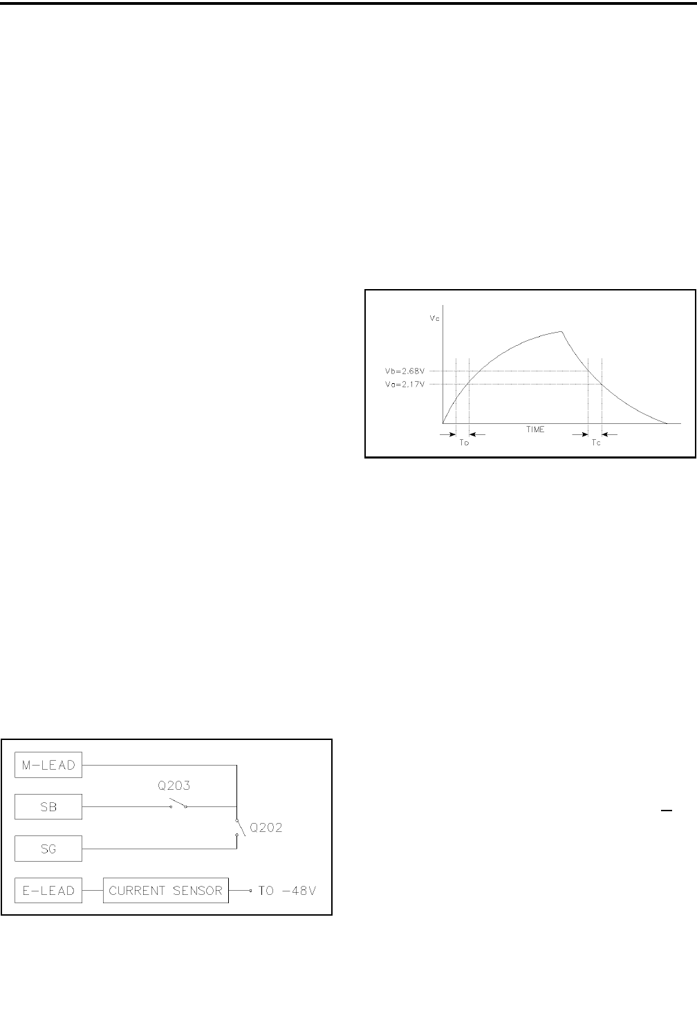
nential ramp voltage on C227. R231/R232 set a refer-
ence of 2.17V and R233/R234 set a reference at 2.86V.
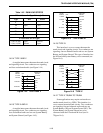
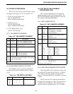
As C227 is charging from 0 to +5V the comparator
sequentially trips causing U213 to trip first and U214
to trip ~ 0.3 ms later (see Figure 14-12).
Figure 14-12 CHARGING CHARACTERISTIC
OF C227
When a "0" is written to Q201 the reverse action
occurs with the discharge of C227 through R230. The
reason for this sequencing is to emulate a "break-
before-make" switch. By sequencing the drive to the
optoisolators U204 becomes an equivalent SPDT
switch. When the output of the comparators goes low,
they activate U213/U214.
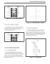
The E-Lead output from U212 is debounced by
dual retriggerable monostable multivibrator U210. It
is configured as two one-shot multivibrators with RC
time constants of 5 ms and 10 ms respectively. This
circuit debounces transients in both E-Lead signal
states (low or high).
The first one-shot multi vibrator is used to
debounce a transient “1” during a logic “0”. The Q
output of the first one-shot is NANDed with its input
(R221/C226 are used to eliminate a possible race
condition that may occur through the one-shot) in
which the output of U211, pin 3 goes low only when
the input pulse width exceeds 5 ms. This output is fed
into U210, pin 12 which is being retriggered by the


