


NETWORK INTERFACE MODULE (NetNIM)
6-2
6.2.1 LEDS
1. Clock A and B LED
Clock A/B LED is on for clock A and off for
clock B.
2. Companion Clock LED
The companion clock LED is on if the companion
card indicates a malfunction or if the companion card
is not installed. Otherwise, the clock(s) are func-
tioning and the LED is off.
3. Comm to SMM LED
The Comm to SMM LED is on if the NIM is the
selected unit to communicate to the SMM. Otherwise,
the LED is off.
4. Alarm LED
The Alarm LED is on if there is a NIM failure.
This is presently done on power-up if there is a RAM
or ROM malfunction.
6.3 SETUP PROCEDURE
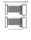
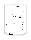
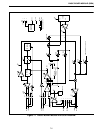
6.3.1 JUMPERS
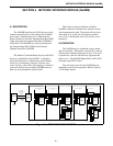
J11 and J12 select the Tx/Rx direction of the SSB
lines. J13 and J14 select the Tx/Rx direction of the
SMB lines. (See Figure 6-3.)
6.3.2 SWITCHES
S1 - Reset
Normally open, press to reset. Momentary switch
used to reset the module.
6.4 ALIGNMENT SPECIFICATIONS
The NetNIM alignment ensures the correct PCM
Clock and Sync frequencies and sets the frequency
detectors.
1. Measure the frequency of clock "A" at TP31 with a
10 MHz counter.
2. Adjust C62 for 4.096 MHz
±200 Hz at TP31.
3. Measure the frequency of U30, pin 1 for 4 kHz
±0.25
Hz
.
4. Measure the frequency of clock "B" at J32 with a 10
MHz counter.
5. Adjust C65 for 4.096 MHz
±200 Hz at TP32.
6. Measure the frequency of U29, pin 1 for 4 kHz
±0.25
Hz.
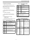
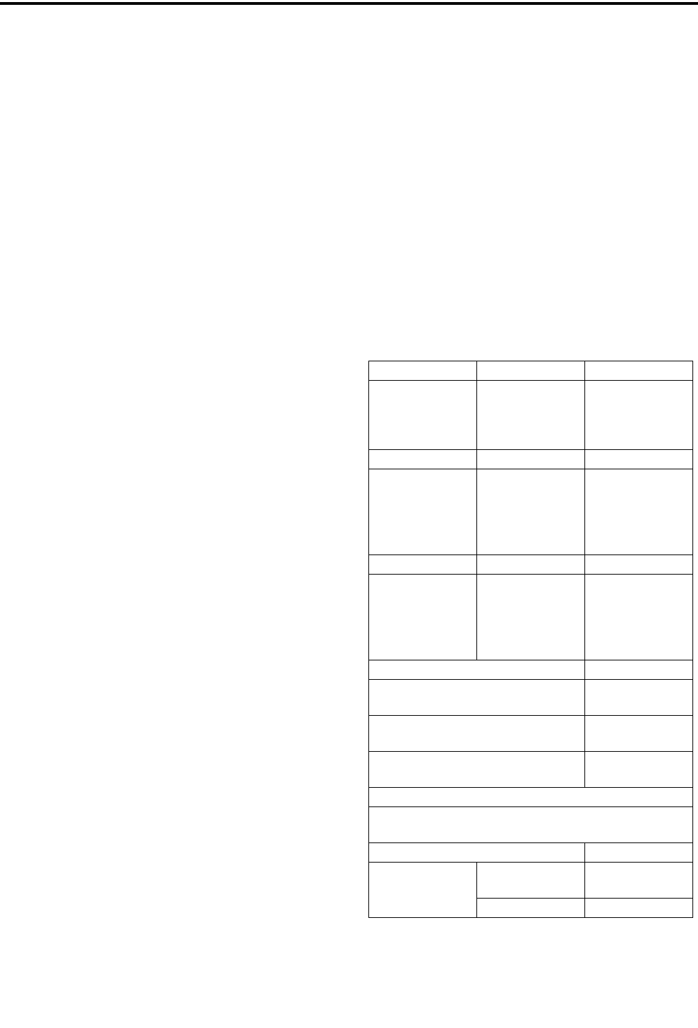
Table 6-1 NIM JUMPERS
Jumpers Pins Bus
J11
J12
J13
J14
1 to 2
1 to 2
1 to 2
1 to 2
NetCSB Rx
NetCSB Tx
NetIDB Rx
NetIDB Tx
NetCSB Pins Baud Rate
J15 1 to 2
3 to 4
5 to 6
7 to 8
9 to 10
19200
9600 (normal)
4800
2400
1200
NetIDB Pins Baud Rate
J16 1 to 2
3 to 4
5 to 6
7 to 8
9 to 10
19200
9600 (normal)
4800
2400
1200
PROM Addressing Addressing
J24-pin 1 to J25-pin 1
J24-pin 2 to J25-pin 2
27256
(normal)
J24-pin 1 to J25-pin 1
J24-pin 3 to J25-pin 3
27128
J24-pin 1 only
J24-pin 3 to J25-pin 3
2764
Watch-Dog Timer Operation
J26 - Not used, jumper is placed on J26-pin 1
only for normal operation.
DCB/CSB Data Bus Select Data Bus
J33 pin 1 to pin 2 Switch CSB (nor-
mal)
pin 2 to pin 3 ACS