


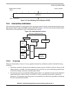
System Control Module (SCM)
MCF52211 ColdFire® Integrated Microcontroller Reference Manual, Rev. 2
12-4 Freescale Semiconductor
NOTE
Accessing reserved IPSBAR memory space could result in an unterminated
bus cycle that causes the core to hang. Only a hard reset allows the core to
recover from this state. Therefore, all bus accesses to IPSBAR space should
fall within a module’s memory map space.
If an address hits in overlapping memory regions, the following priority is used to determine what memory
is accessed:
1. IPSBAR
2. RAMBAR
NOTE
This is the list of memory access priorities when viewed from the processor
core.
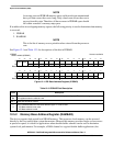
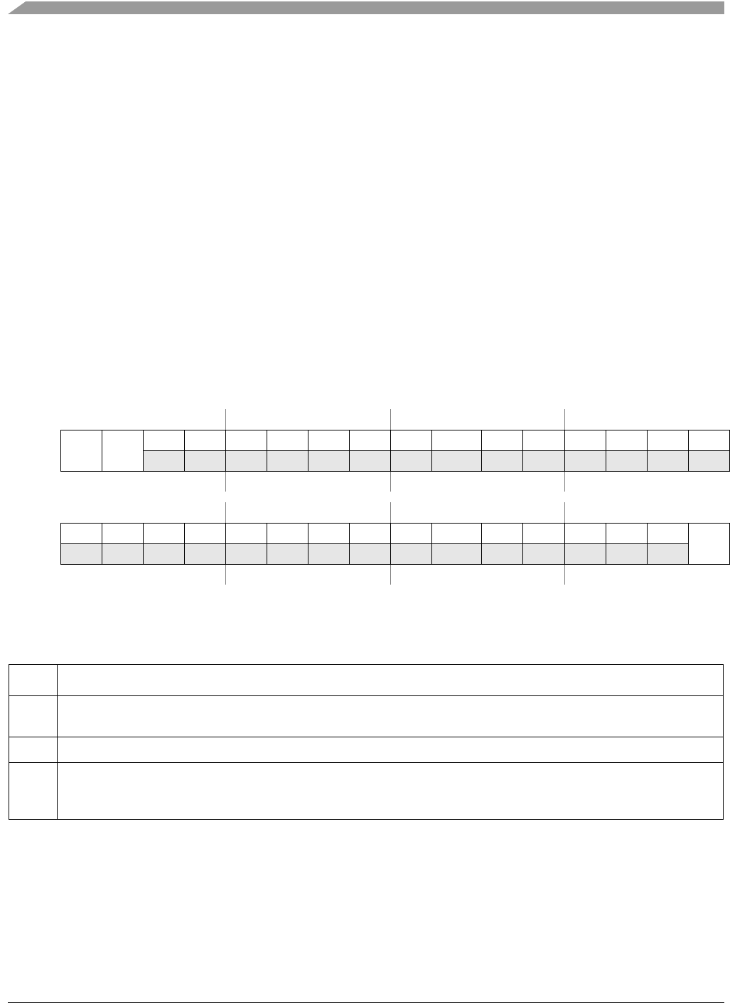
See Figure 12-1 and Table 12-3 for descriptions of the bits in IPSBAR.
12.5.2 Memory Base Address Register (RAMBAR)
The device supports dual-ported local SRAM memory. This processor-local memory can be accessed
directly by the core and/or other system bus masters. Because this memory provides single-cycle accesses
at processor speed, it is ideal for applications where double-buffer schemes can be used to maximize
system-level performance. For example, a DMA channel in a typical double-buffer application (also
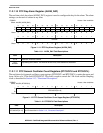
IPSBAR
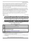
Offset: 0x0000 (IPSBAR)
Access: read/write
31 30 29 28 27 26 25 24 23 22 21 20 19 18 17 16
R
BA31 BA30
0 0 0 0000 0 000 000
W
Reset010000000 0 000000
15 14 13 12 11 10 9 8 7 6 5 4 3 2 1 0
R 0 00000000 0 00000
V
W
Reset000000000 0 000001
Figure 12-1. IPS Base Address Register (IPSBAR)
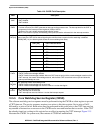
Table 12-3. IPSBAR Field Description
Field Description
31–30
BA
Base address. Defines the base address of the 1-Gbyte internal peripheral space. This is the starting address for the
IPS registers when the valid bit is set.
29–1 Reserved, should be cleared.
0
V
Valid. Enables/disables the IPS Base address region. V is set at reset.
0 IPS Base address is not valid.
1 IPS Base address is valid.