


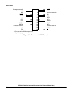
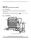

IEEE 1149.1 Test Access Port (JTAG)
MCF52211 ColdFire® Integrated Microcontroller Reference Manual, Rev. 2
Freescale Semiconductor 29-3
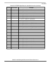
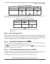
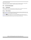
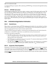
When one module is selected, the inputs into the other module are disabled or forced to a known logic
level, as shown in Table 29-3, to disable the corresponding module.
NOTE
The JTAG_EN does not support dynamic switching between JTAG and
BDM modes.
29.2.2 Test Clock Input (TCLK)
The TCLK pin is a dedicated JTAG clock input to synchronize the test logic. Pulses on TCLK shift data
and instructions into the TDI pin on the rising edge and out of the TDO pin on the falling edge. TCLK is
independent of the processor clock. The TCLK pin has an internal pull-up resistor, and holding TCLK high
or low for an indefinite period does not cause JTAG test logic to lose state information.
29.2.3 Test Mode Select/Breakpoint (TMS/BKPT)
The TMS pin is the test mode select input that sequences the TAP state machine. TMS is sampled on the
rising edge of TCLK. The TMS pin has an internal pull-up resistor.
The BKPT
pin is used to request an external breakpoint. Assertion of BKPT puts the processor into a halted
state after the current instruction completes.
29.2.4 Test Data Input/Development Serial Input (TDI/DSI)
The TDI pin receives serial test and data, which is sampled on the rising edge of TCLK. Register values
are shifted in least significant bit (lsb) first. The TDI pin has an internal pull-up resistor.
The DSI pin provides data input for the debug module serial communication port.
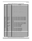
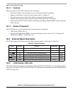
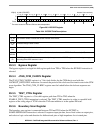
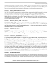
Table 29-2. Pin Function Selected
JTAG_EN = 0 JTAG_EN = 1 Pin Name
Module selected BDM JTAG —
Pin Function —
BKPT
DSI
DSO
DSCLK
TCLK
TMS
TDI
TDO
TRST
TCLK
BKPT
DSI
DSO
DSCLK
Table 29-3. Signal State to the Disable Module
JTAG_EN = 0 JTAG_EN = 1
Disabling JTAG TRST
= 0
TMS = 1
—
Disabling BDM — Disable DSCLK
DSI = 0
BKPT
= 1