


DMA Timers (DTIM0–DTIM3)
MCF52211 ColdFire® Integrated Microcontroller Reference Manual, Rev. 2
22-2 Freescale Semiconductor
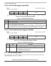
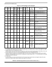
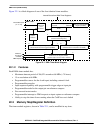
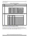
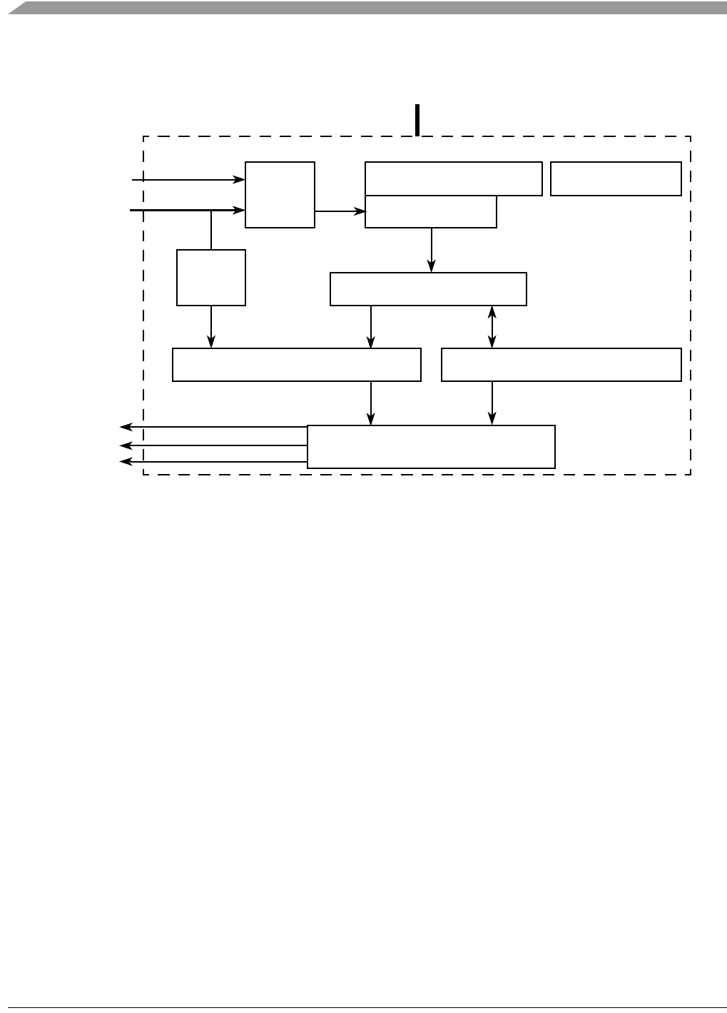
Figure 22-1 is a block diagram of one of the four identical timer modules.
Figure 22-1. DMA Timer Block Diagram
22.1.2 Features
Each DMA timer module has:
• Maximum timeout period of 266,521 seconds at 66 MHz (~74 hours)
• 15-ns resolution at 66 MHz
• Programmable sources for the clock input, including external clock
• Programmable prescaler
• Input-capture capability with programmable trigger edge on input pin
• Programmable mode for the output pin on reference compare
• Free run and restart modes
• Programmable interrupt or DMA request on input capture or reference-compare
• Ability to stop the timer from counting when the ColdFire core is halted
22.2 Memory Map/Register Definition
The timer module registers, shown in Table 22-1, can be modified at any time.
DMA Timer
Divider
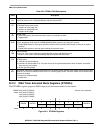
DMA Timer Mode Register (DTMRn)
Prescaler Mode Bits
DMA Timer Counter Register (DTCNn)
31 0
DMA Timer Reference Register (DTRRn)
31 0
DMA Timer Capture Register (DTCRn)
31 0
DMA Timer Event Register (DTERn)
Capture
Detection
clock
(contains incrementing value)
(reference value for comparison with DTCN)
(indicates capture or when DTCN = DTRRn)
To Interrupt
Clock
Generator
DMA Timer Extended Mode
Register (DTXMRn)
DMA Request
0
0
15
7
7
0
controller
Internal Bus Clock
(÷1 or ÷16
)
DMA Timer
Internal Bus to/from DMA Timer Registers
(latches DTCN value when triggered byDTINn)
DTOUTn