


Debug Module
MCF52211 ColdFire® Integrated Microcontroller Reference Manual, Rev. 2
Freescale Semiconductor 28-37
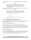
else A7 = User Stack Pointer
OTHER_A7 = Supervisor Stack Pointer
The BDM programming model supports reads and writes to A7 and OTHER_A7 directly. It is the
responsibility of the external development system to determine the mapping of A7 and OTHER_A7 to the
two program-visible definitions (supervisor and user stack pointers), based on the SR[S] bit.
28.5.3.3.12 Write Control Register (WCREG)
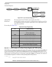
The operand (longword) data is written to the specified control register. The write alters all 32 register bits.
See the RCREG instruction description for the Rc encoding and for additional notes on writes to the A7
stack pointers and the EMAC programming model.
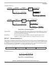
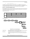
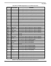
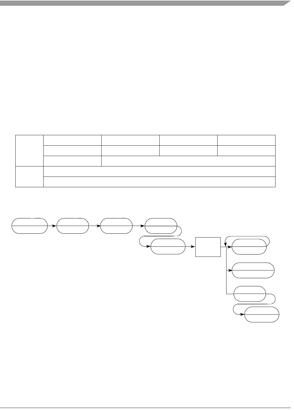
Command/Result Formats:
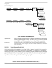
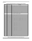
Command Sequence:
Figure 28-39. WCREG Command Sequence
Operand Data: This instruction requires two longword operands. The first selects the register to
the operand data writes to; the second contains the data.
Result Data: Successful write operations return 0xFFFF. Bus errors on the write cycle are
indicated by the setting of bit 16 in the status message and by a data pattern of
0x0001.
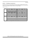
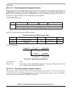
1514131211109876543210
Command 0x2 0x8 0x8 0x0
0x0 0x0 0x0 0x0
0x0 Rc
Result D[31:16]
D[15:0]
Figure 28-38. WCREG Command/Result Formats
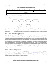
XXX
’NOT READY’
WCREG
???
MS ADDR
’NOT READY’
MS ADDR
’NOT READY’
WRITE
CONTROL
REGISTER
NEXT CMD
’CMD COMPLETE’
MS DATA
’NOT READY’
NEXT CMD
’NOT READY’
XXX
BERR
LS DATA
’NOT READY’