


Static RAM (SRAM)
MCF52211 ColdFire® Integrated Microcontroller Reference Manual, Rev. 2
5-2 Freescale Semiconductor
5.2.1 SRAM Base Address Register (RAMBAR)
The configuration information in the SRAM base-address register (RAMBAR) controls the operation of
the SRAM module.
• The RAMBAR holds the SRAM base address. The MOVEC instruction provides write-only access
to this register.
• The RAMBAR can be read or written from the debug module.
• All undefined bits in the register are reserved. These bits are ignored during writes to the
RAMBAR and return zeroes when read from the debug module.
• A reset clears the RAMBAR’s valid bit. This invalidates the processor port to the SRAM (The
RAMBAR must be initialized before the core can access the SRAM.) All other bits are unaffected.
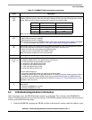
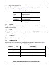
The RAMBAR contains several control fields. These fields are shown in Figure 5-1.
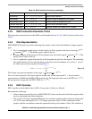
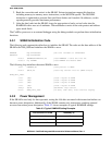
Table 5-1. SRAM Programming Model
Rc[11:0]
1
1
The values listed in this column represent the Rc field used when accessing the core registers via the BDM port. For more
information see Chapter 28, “Debug Module.”
Register
Width
(bits)
Access Reset Value
Written
w/ MOVEC
Section/Page
Supervisor Access Only Registers
0xC05 RAM Base Address Register (RAMBAR) 32 R/W See Section Yes 5.2.1/5-2
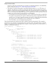
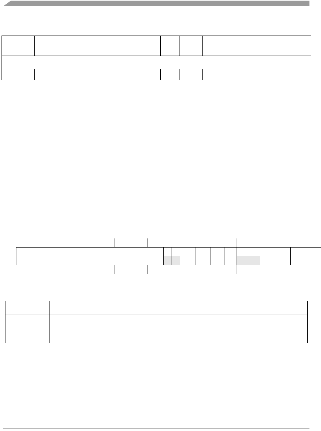
Rc[11:0]: 0x0C05 (RAMBAR) Access: User write-only
Debug read/write
31 30 29 28 27 26 25 24 23 22 21 20 19 18 17 16 15 14 13 12 11 10 9 8 7 6 5 4 3 2 1 0
R
BA
0 0
PRIU PRIL SPV WP
0 0
C/I SC SD UC UD V
W
ResetUUUUUUUUUUUUUUUUUUUU 0 0 0 U 0 0 U U U U U 0
Figure 5-1. SRAM Base Address Register (RAMBAR)
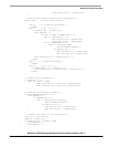
Table 5-2. RAMBAR Field Descriptions
Field Description
31–14
BA
Base Address. Defines the 0-modulo-32K base address of the SRAM module. By programming this field,
the SRAM may be located on any 32-Kbyte boundary.
13–12 Reserved, should be cleared.