


Debug Module
MCF52211 ColdFire® Integrated Microcontroller Reference Manual, Rev. 2
28-6 Freescale Semiconductor
28.4 Memory Map/Register Definition
In addition to the existing BDM commands that provide access to the processor’s registers and the memory
subsystem, the debug module contain a number of registers to support the required functionality. These
registers are also accessible from the processor’s supervisor programming model by executing the
WDEBUG instruction (write only). Therefore, the breakpoint hardware in debug module can be read or
written by the external development system using the debug serial interface or written by the operating
system running on the processor core. Software guarantees that accesses to these resources are serialized
and logically consistent. Hardware provides a locking mechanism in CSR to allow external development
system to disable any attempted writes by the processor to the breakpoint registers (setting CSR[IPW]).
BDM commands must not be issued if the ColdFire processor is using the WDEBUG instruction to access
debug module registers, or the resulting behavior is undefined. The DSCLK must be quiescent during
operation of the WDEBUG command.
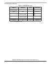
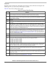
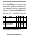
These registers, shown in Table 28-4, are treated as 32-bit quantities, regardless of the number of
implemented bits. These registers are also accessed through the BDM port by the commands, WDMREG
and RDMREG, described in Section 28.5.3.3, “Command Set Descriptions”. These commands contain a
5-bit field, DRc, that specifies the register, as shown in Table 28-4.
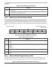
Table 28-4. Debug Module Memory Map
DRc[4–0] Register Name
Width
(bits)
Access Reset Value
Section/
Page
0x00 Configuration/status register (CSR) 32 R/W
See Note
0x0090_0000 28.4.2/28-7
0x05 BDM address attribute register (BAAR) 32
1
1
Each debug register is accessed as a 32-bit register; reserved fields are not used (don’t care).
W 0x05 28.4.3/28-10
0x06 Address attribute trigger register (AATR) 32
1
W 0x0005 28.4.4/28-10
0x07 Trigger definition register (TDR) 32 W 0x0000_0000 28.4.5/28-12
0x08 PC breakpoint register 0 (PBR0) 32 W Undefined 28.4.6/28-15
0x09 PC breakpoint mask register (PBMR) 32 W Undefined 28.4.6/28-15
0x0C Address breakpoint high register (ABHR) 32 W Undefined 28.4.7/28-17
0x0D Address breakpoint low register (ABLR) 32 W Undefined 28.4.7/28-17
0x0E Data breakpoint register (DBR) 32 W Undefined 28.4.8/28-18
0x0F Data breakpoint mask register (DBMR) 32 W Undefined 28.4.8/28-18
0x18 PC breakpoint register 1 (PBR1) 32 W See Section 28.4.6/28-15
0x1A PC breakpoint register 2 (PBR2) 32 W See Section 28.4.6/28-15
0x1B PC breakpoint register 3 (PBR3) 32 W See Section 28.4.6/28-15