


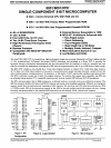
8051
Architectural Specification and Functional Description
updated to a one (1), a pin programmed as
an
input will
not
source current into the
TTL
gate
that
is driving
it
if
the
pin is
later written with
another
one (1). Since
the
quasi-
bidirectional
output
driver sources current for only two
oscillator periods,
an
internal pullup resistor
of
ap-
proximately 20K- to 4OK-ohms
is
provided to hold the
external
driver's loading
at
a
TTL
high level. Ports
1,
2
and
3 can sink/ source one TTL load.
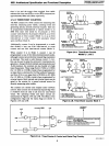
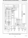
2.1.2.2.3
Microprocessor
Bus
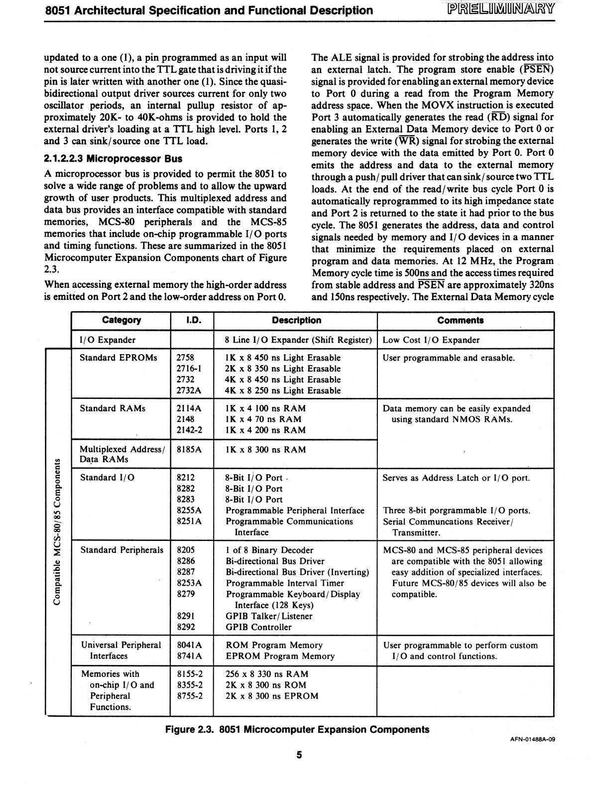
A microprocessor bus is provided to permit the
80S
1
to
solve a wide range
of
problems
and
to allow the upward
growth
of
user products. This multiplexed address
and
data
bus provides
an
interface compatible with standard
memories,
MCS-80 peripherals
and
the MCS-8S
memories
that
include on-chip programmable
I/O
ports
and
timing functions. These are summarized in the
80S
1
Microcomputer Expansion Components
chart
of
Figure
2.3.
When accessing external memory the high-order address
is
emitted
on
Port
2
and
the low-order address
on
Port
O.
The ALE signal is provided
for
strobing the address into
an
external latch.
The
program store enable (PSEN)
signal is provided for enabling
an
external memory device
to
Port
0 during a read from the Program Memory
address space. When the
MOVX instruction is executed
Port
3 automatically generates the read
(RD)
signal
for
enabling
an
External
Data
Memory device
to
Port
0
or
generates the write
(WR)
signal for strobing the external
memory device with the
data
emitted by
Port
O.
Port
0
emits the address
and
data
to
the external memory
through a push/ pull driver
that
can sink/ source two
TTL
loads. At the end
of
the read/write bus cycle
Port
0 is
automatically reprogrammed
to
its high impedance state
and
Port
2 is returned
to
the state it had
prior
to
the bus
cycle. The
80S
1 generates the address,
data
and
control
signals needed by memory
and
I/O
devices in a manner
that
minimize the requirements placed
on
external
program and
data
memories.
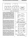
At
12
MHz, the Program
Memory cycle time is
SOOns
and
the access times required
from stable address
and
PSEN
are
approximately 320ns
and
lSOns
respectively. The External
Data
Memory cycle
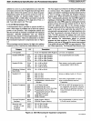
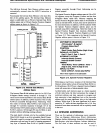
Category
1.0.
Description
Comments
I/O
Expander
8 Line
I/O
Expander (Shift Register)
Low Cost
I/O
Expander
Standard
EPROMs
2758 I K x 8 450 ns Light Erasable
User programmable
and
erasable.
2716-1 2K x 8 350 ns Light Erasable
2732
4K x 8 450 ns Light Erasable
2732A
4K
x 8 250 ns Light Erasable
Standard
RAMs 2114A
IK
x 4
100
ns
RAM
Data
memory can be easily expanded
2148
lK
x 4 70 ns
RAM
using standard
NMOS
RAMs.
2142-2
I K x 4
200 ns
RAM
Multiplexed Address/
8185A
I K x 8
300
ns
RAM
'"
Da.ta
RAMs
C
'"
Standard
I/O
8-Bit Ii 0
Port
.
c
8212
Serves as Address Latch
or
I/O
port.
0
Q,
8282
8-Bit
I/O
Port
e
0
8283
8-Bit
I/O
Port
U
on
8255A Programmable Peripheral Interface Three 8-bit porgrammable
I/O
ports.
QO
8251
A
Programmable Communications
Serial Communcations Receiver/
Q
QO
Interface
Transmitter .
•
ell
U
Standard
Peripherals 8205
I
of
8 Binary Decoder MCS-80 and MCS-85 peripheral devices
~
'"
8286
Bi-directional Bus Driver are compatible with the
8051·
allowing
;§
8287
Bi-directional Bus Driver (Inverting) easy addition
of
specialized interfaces.
;
Q,
8253A
Programmable Interval Timer
Future
MCS-80/85 devices will also be
e
8279
Programmable Keyboard/ Display compatible.
0
U
Interface (128 Keys)
8291
GPIB
Talker/Listener
8292
GPIB Controller
Universal Peripheral
8041
A
ROM
Program
Memory User programmable to perform custom
Interfaces 8741A
EPROM
Program
Memory
I/O
and control functions.
Memories with
8155-2
256 x 8 330 ns
RAM
on-chip
I/O
and
8355-2 2K x 8 300 ns ROM
Peripheral 8755-2
2K x 8
300 ns
EPROM
Functions.
Figure 2.3.
8051
Microcomputer Expansion Components
AFN-Q1488A-09
5