


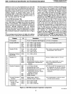
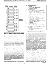
8051
Architectural Specification and Functional Description
processing
is
especially effective in systems where controls
in a complex process are required
at
physically separated
locations.
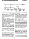
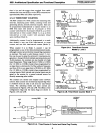
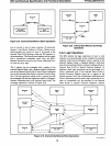
In Modes 2
and
3 the automatic wake-up of slave
processors through interrupt driven address-frame
recognition
is
provided
to
facilitate interprocessor com-
munications. The protocol for interprocessor com-
munications
is
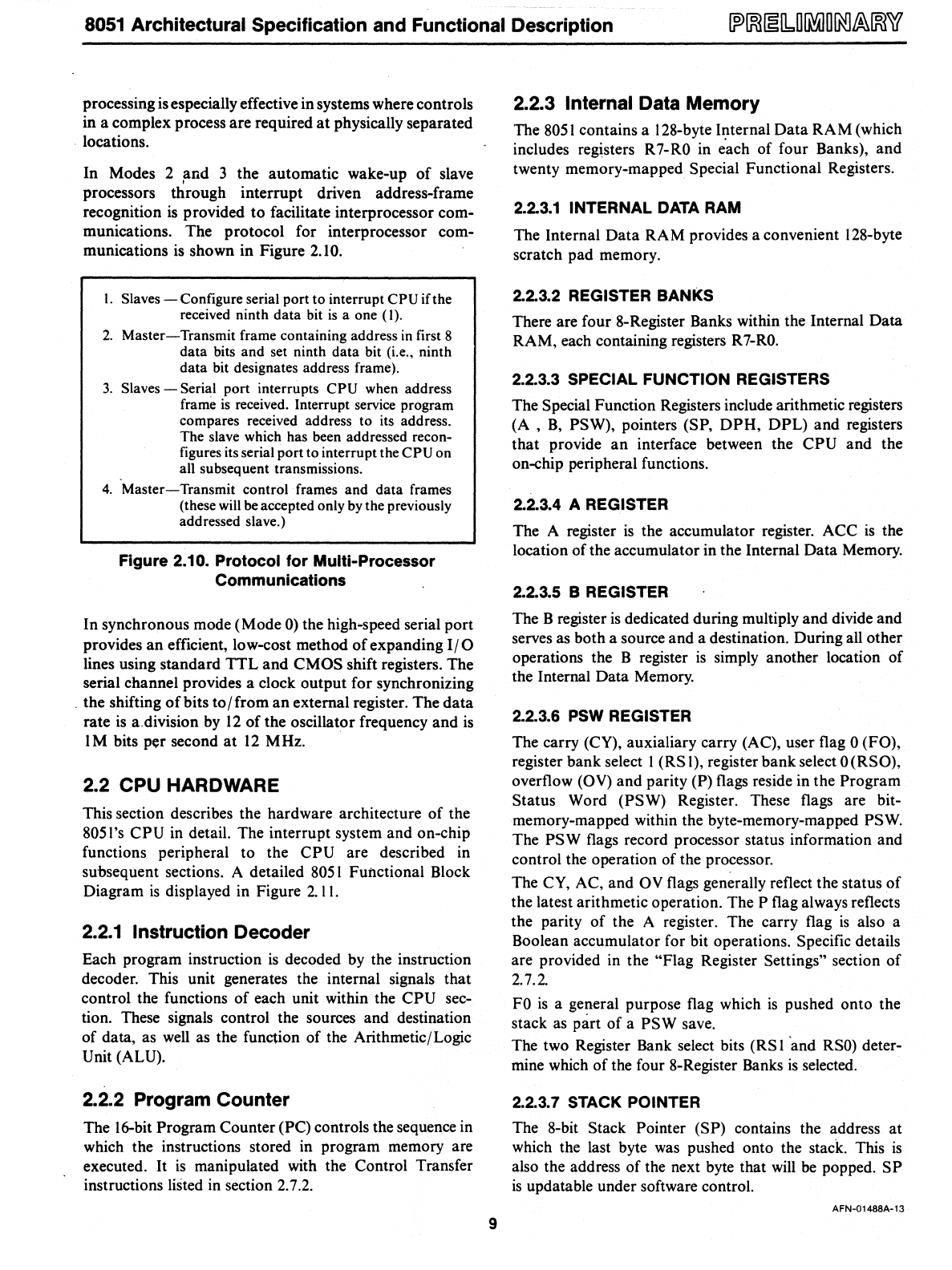
shown in Figure 2.10.
1.
Slaves
-Configure
serial
port
to
interrupt
CPU
if the
received ninth
data
bit
is
a one (I).
2.
Master-Transmit
frame containing address in first 8
data
bits
and
set ninth
data
bit (i.e., ninth
data
bit designates address frame).
3.
Slaves - Serial port interrupts
CPU
when address
frame
is
received. Interrupt service program
compares received address to its address.
The slave which has been addressed recon-
figures its serial
port
to interrupt the
CPU
on
all subsequent transmissions.
4.
Master-Transmit
control frames and
data
frames
(these will
be
accepted only by the previously
addressed slave.)
Figure 2.10. Protocol for Multi-Processor
Communications
In synchronous mode (Mode
0)
the high-speed serial port
provides
an
efficient, low-cost method
of
expanding
I/O
lines using standard
TTL
and CMOS shift registers. The
serial channel provides a clock output for synchronizing
. the shifting
of
bits
to/from
an
external register. The
data
rate
is
a.division
by
12
of the oscillator frequency
and
is
I M bits
p(:r
second
at
12
MHz.
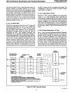
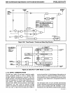
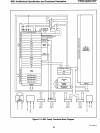
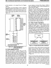
2.2 CPU HARDWARE
This section describes the hardware architecture of the
8051's
CPU
in
detaiL The interrupt system and on-chip
functions peripheral to the
CPU are described
in
subsequent sections. A detailed
8051
Functional Block
Diagram
is
displayed in Figure
2.
II.
2.2.1
Instruction Decoder
Each program instruction
is
decoded by the instruction
decoder. This unit generates the internal signals that
control the functions of each unit within the
CPU sec-
tion. These signals control the sources and destination
of data, as
well
as the function of the Arithmetic/Logic
Unit (ALU).
2.2.2 Program Counter
The I6-bit Program Counter (PC) controls the sequence in
which the instructions stored in program memory are
executed.
It
is
manipulated with the Control Transfer
instructions listed in section 2.7.2.
9
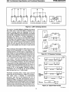
2.2.3 Internal Data Memory
The
8051
contains a I 28-byte Internal
Data
RAM
(which
includes registers
R7-RO
in e'ach of four Banks), and
twenty memory-mapped
Special Functional Registers.
2.2.3.1 INTERNAL
DATA
RAM
The Internal
Data
RAM provides a convenient 128-byte
scratch pad memory.
2.2.3.2 REGISTER BANKS
There are four 8-Register Banks within the Internal Data
RAM, each containing registers
R7-RO.
2.2.3.3 SPECIAL
FUNCTION
REGISTERS
The Special Function Registers include arithmetic registers
(A ,
B,
PSW), pointers (SP,
DPH,
DPL) and registers
that provide
an
interface between the CPU and the
on-chip peripheral functions.
2.2.3.4 A REGISTER
The A register
is
the accumulator register. ACC
is
the
location
of
the accumulator in the Internal Data Memory.
2.2.3.5 B REGISTER
The B register
is
dedicated during multiply and divide and
serves as both a source and a destination. During all other
operations the B register
is
simply another location of
the Internal Data Memory.
2.2.3.6 PSW REGISTER
The carry (CY), auxialiary carry (AC), user flag 0 (FO),
register bank select I (RS I), register bank select 0 (RSO),
overflow (OV) and parity (P) flags reside in the Program
Status Word (PSW) Register. These flags are bit-
memory-mapped within the byte-memory-mapped
PSW.
The PSW flags record processor status information and
control the operation of the processor.
The CY, AC, and
OV
flags generally reflect the status of
the latest arithmetic operation. The P flag
always reflects
the parity of the A register. The carry flag
is
also a
Boolean accumulator for bit operations.
Specific details
are provided in the
"Flag Register Settings" section
of
2.7.2.
FO
is
a general purpose flag which
is
pushed onto the
stack as
part
of
a PSW save.
The two Register Bank select bits
(RS I 'and
RSO)
deter-
mine which of the four 8-Register Banks
is
selected.
2.2.3.7 STACK POINTER
The 8-bit Stack Pointer (SP) contains the address at
which the last byte
was
pushed onto the stack. This
is
also the address of the next byte that
will
be
popped.
SP
is
updatable under software control.
AFN·01488A-13