


8051
Architectural Specification and Functional Description
8031/8051/8751
SINGLE-COMPONENT 8-BIT MICROCOMPUTER
•
803t
- Control Oriented CPU With RAM and
I/O
•
8051
- An
8031
With Factory Mask- Programmable ROM
•
8751
-
An
8031
With User Programmable/Erasable EPROM
• 4K x 8 ROM/EPROM
• 128 x 8 RAM
• Four 8-Bit Ports, 32 I/O Lines
• Two 16-Bit Timer/Event Counters
• High-Performance Full-Duplex Serial
Channel
• Boolean Processor
•
Compatible
with
MCS-80™/MCS-85TM
Peripherals
• External
Memory
Expandable
to
128K
• MCS-48™ Architecture Enhanced with:
• Non-Paged Jumps
• Direct Addressing
• Four 8-Register Banks
• Stack Depth
Up
to 128-Bytes
• Multiply, Divide, Subtract, Compare
• Most Instructions Execute
in
111S
•
411s
Multiply
and Divide
The Intel® 8031/8051/8751
is
a stand-alone, high-performance single-chip computer fabricated with Intel's highly-reliable
+5
Volt, depletion-load, N-Channel, silicon-gate HMOS technology and packaged in a 40-pin DIP. It provides the
hardware features, architectural enhancements and new instructions that are necessary to make
it
a powerful and cost
effective controller for applications requiring up to 64K bytes
of
program memory and /
or
up to 64K bytes
of
data
storage.
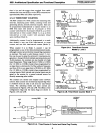
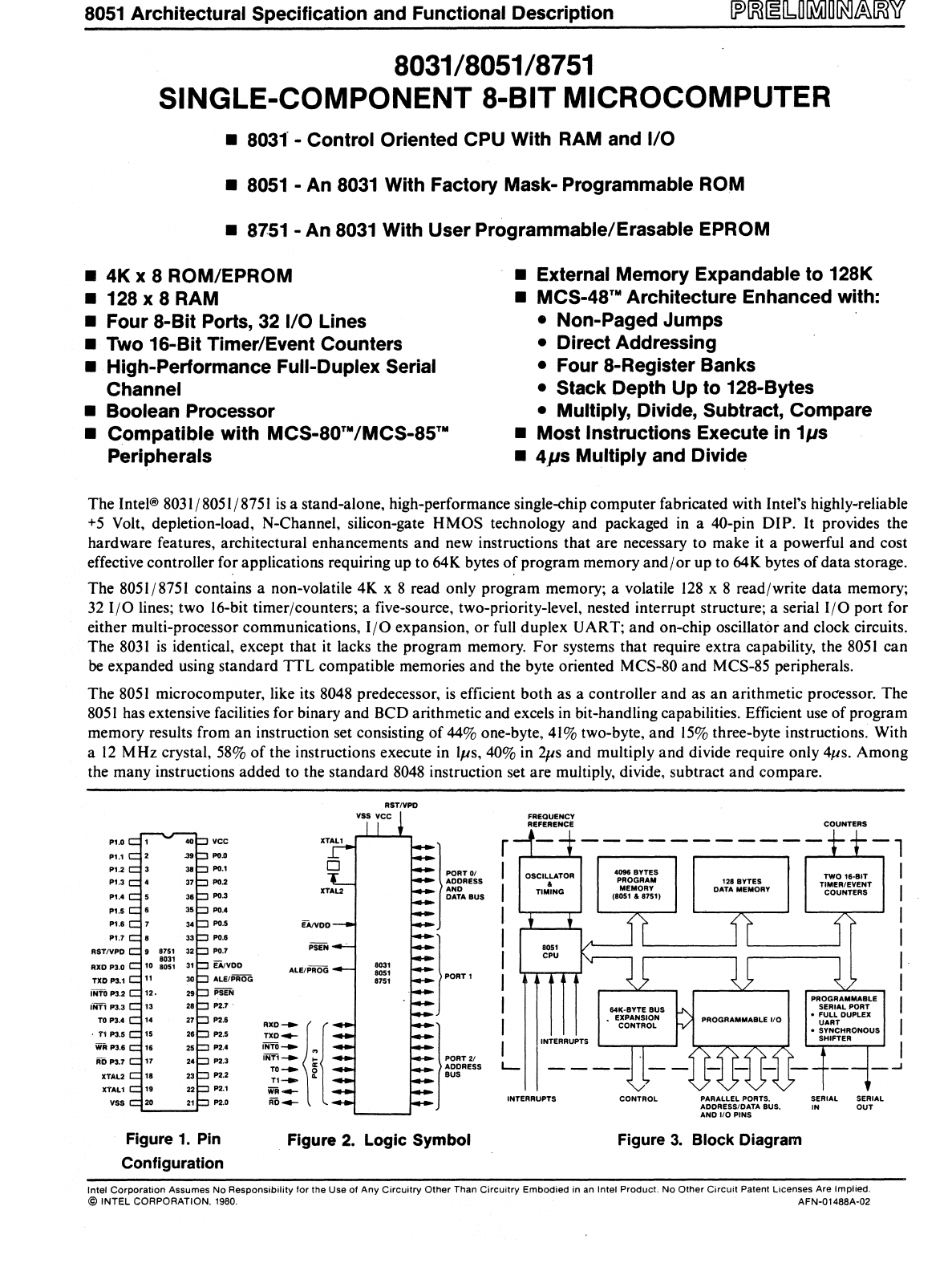
The
8051/8751 contains a non-volatile 4K x 8 read only program memory; a volatile
128
x 8 read/write data memory;
32
I/O
lines; two 16-bit timer/counters; a five-source, two-priority-Ievel, nested interrupt structure; a serial
I/O
port for
either multi-processor communications,
I/O
expansion,
or
full duplex UART; and on-chip oscillator and clock circuits.
The
8031
is
identical, except that
it
lacks the program memory.
For
systems that require extra capability, the
8051
can
be
expanded using standard TTL compatible memories and the byte oriented MCS-80 and MCS-85 peripherals.
The
8051
microcomputer, like its 8048 predecessor,
is
efficient both as a controller and as an arithmetic processor. The
8051
has extensive facilities for binary and BCD arithmetic and excels in bit-handling capabilities. Efficient
use
of
program
memory results from
an
instruction set consisting
of
44% one-byte,
41%
two-byte, and
15%
three-byte instructions. With
a
12
MHz crystal, 58%
of
the instructions execute in Ills, 40% in
2f1s
and mUltiply and divide require only
411S.
Among
the many instructions added to the standard
8048 instruction set are multiply, divide, subtract and compare.
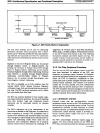
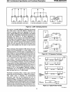
AST/VPD
FREQUENCY
REFERENCE
COUNTERS
P1.0
vee
P1,1
PO.o
}-.
r
I
I
I
I
I
I
I
I
-1
,...----'---'---,
P1.2
PO.1
P1.3
PO.2
P1.4
PO.3
P1.5
PO.4
P1.6
PO.S
P1.7
PO.S
RST/VPO
PO.7
RXD P3.0
EAtVDO
TXO P3.1
ALEIPROG
INTO P3.2
PSEN
uin
P3.3
P2.7
TO
P3.4
P2.S
T1
P3.5 P2.5
\VA
P3.6
P2."
RD
P3.7
P2.3
XTAL2
P2.2
XTAL1
P2.1
VSS
P2.D
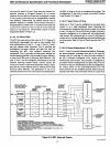
Figure
1.
Pin
Configuration
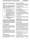
ADDRESS
AND
OATA
BUS
}-,
PSEN
ALE/PROG
.m_
{{
TXO
.....
INTO
......
INT'......
:
}~"'.
TO-'
g
ADDRESS
n........
Q.
BUS
WA~
AD"-
Figure 2.
Logic
Symbol
I
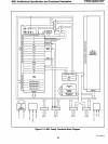
INTERRUPTS
L-
INTERRUPTS
64K-SYTE
8US
•
EXPANSION
CONTROL
CONTROL
128
BYTES
DATA
MEMORY
PARALLEL
PORTS.
ADDRESS/DATA
BUS,
AND
110
PINS
Figure
3.
Block Diagram
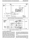
TWO
16-BIT
TIMER/EVENT
COUNTERS
PROGRAMMABLE
SERIAL
PORT
•
FULL
DUPLEX
UART
•
SYNCHRONOUS
SHIFTER
SERIAL SERIAL
IN
OUT
Intel
Corporation
Assumes
No
Responsibility
for
the
Use
of
Any
Circuitry
Other
Than
Circuitry
Embodied
in
an Intel
Product.
No
Other
Circuit
Patent
licenses
Are
Implied.
© INTEL CORPORATION.
1980.
AFN-01488A-02
I
I
I
I
I
I
I
I
I