


tsU~l
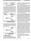
ArcnneCtural :specification and Functional Description
the
8051
fetches instructions from internal Program
Memory when the address
is
between 0 and 4095 and
from external Program Memory when the addressed
memory location
is
between 4096 and 64K. In either case,
Ports 2 and
0 are automatically configured as an external
bus based on the value
of
the
Pc.
Instruction
executio[}o
times are the same for code fetched from internal or
external Program Memory.
Up to 64K
of
External Data Memory can
be
accessed
using the
MOVX instructions. These instructions auto-
matically configure
Port
0, and often Port
2,
as an
external bus. The
MOVX instructions
use
the DPTR,
RI
or
RO
register as a pointer into the External Data
Memory. The 16-bit
DPTR
register
is
used when succes-
sive accesses cover a wide range of the 64K space. The
8-bit
Rl
and
RO
registers provide greatest byte efficiency
when successive accesses are constrained to a 256-byte
block of the External Data Memory space. When using
Rl
and
RO
a subsequent block can be accessed
by
updating
the output latch of Port.
2.
Port 2
is
not affected by
execution
of
a MOVX that
uses
Rl
or
RO
such that, if
32K or less
of
external memory
is
present, only part
of
Port 2 needs to
be
used for selecting the desired block;
the remaining pins can be used for
I/O.
When a MOVX
using
DPTR
is
executed, the value in Port
2's
output
latch
is
altered only during the external access and then
is
returned to its prior value. This permits efficient exter-
nal block moves by interleaving MOVX instructions that
use
DPTR
and
Rl
or
RO.
The ALE signal
is
generated every sixth oscillator period
during reads from either internal or external Program
Memory. The
PSEN signal
is
generated every sixth oscil-
lator period when reading from the external Program
Memory. When a read
or
write from External Data
Memory
is
being performed, a single ALE and a
RD
or
a
WR signal
is
generated during a twelve oscillator period
interval. The
8051
always fetches an even number of bytes
from its Program Memory.
If
an odd number of bytes
are executed prior to a branch or to an External Data
Memory access, the non-executed byte
is
ignored by the
8051.
If
an instruction requires more oscillator periods
for its execution than for its fetch, the first byte of the
next instruction
is
fetched repeatedly while the first
instruction completes execution.
If
the
CPU
does not
address External Data Memory then ALE
is
generated
every sixth oscillator period and can
be
used as an
external clock. When External Data Memory
is
present,
external logic may
be
used to combine the occurence
of
RD, WR, and ALE to generate an external clock with a
period equal to six oscillator periods.
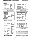
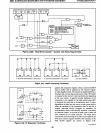
2.10.1
Accessing External
Memory-Opera-
tion of Ports
The Port 0 bus
is
time mUltiplexed to permit transfer
of
both addresses and data. This bus
is
used directly
by
memory and peripheral devices that incorporate on-chip
26
address latching (MCS-85 memories with peripherals),
or
it can be demultiplexed with an address latch
to
generate a non-multiple?Ced bus (MCS-80 peripherals
and memory). During an external access the low-order
byte
of
the address and the
data
(for a write)
is
emitted
by the Port
0 output drivers. Ones (l's) are automatically
written to Port
0
at
the very end of the bus cycle. Since
the Port Ooutput latches will contain ones (I 's) at the end of
the bus cycle, Port
0 will
be
in its high impedance state
when a bus cycle
is
not
in
progress. Port 2 emits the upper
8-bits
of
the address when a MOVX instruction using
DPTR
is
executed. Port
2's
output drivers provide source
current for two oscillator periods when emitting the
address. Port
2's
internal pullup resistors sustain the high
level.
2.10.2 Accessing External
Memory-Bus
Cycle Timing
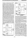
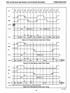
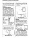
Program Memory Read Sequence (Figure 2.11)
Each Program Memory bus cycle consists
of
six oscil-
lator periods. These are referred to as
n,
T2, T3, T4, T5
and T6 on Figure 2.41. The address
is
emitted from the
processor during T3. Data transfer occurs on the bus
during T5, T6 and the following bus cycle's
Tl.
When
fetching from external Program Memory, the
8051
will
always fetch an even number of bytes.
If
an
odd number
of bytes are executed prior to a branch
or
an External
Data
Memory access the non-executed byte will be
ignored
by
the
8051.
An even number of idle bus cycles
(each 6 oscillator periods in duration) can occur between
external bus cycles when the processor
is
fetching from
internal Program Memory. The read cycle begins during
T2, with the assertion of address latch enable signal ALE
CD
. The falling edge
of
ALE
(3)
is
used to latch the
address information, which
is
present on the bus at this
time
CD
,into
the 8282 latch if a non-multiplexed bus
is
required. At T5, the address
is
removed from the
Port
0
bus and the processor's bus drivers go to the high-
impedance
sta~
. The program memory read
control signal (PSEN)
CD
is
also asserted during T5.
PSEN causes the addressed device to enable its bus
drivers to the now-released bus. At some later time, valid
instruction data will become available on the bus
G)
When the
8051
subsequently returns PSEN to the high
level
(})
• the addressed device will then float its bus
drivers, relinquishing the bus
again®.
For the MOVC instruction the op-code
is
fetched in the
first six-oscillator period, the first byte of the next
in-
struction
is
fetched during the second six-oscillator per-
iod, the table entry
is
fetched
in
a third six-oscillator
period and the first byte of the next instruction
is
again
fetched
in
the fourth six-oscillator period.
Data Memory Read Sequence (Figure 2.42)
Each External Data Memory bus cycle consists of twelve
oscillator periods. These are shown as T I through T
12
on
AFN-Ol488A-30