


8051
Architectural Specification and Functional Description
The silicon economic architecture of the
8048
causes
some inconvenience to the programmer but the relatively
short programs (one or two kilobytes) keep frustration
levels in check. The
8051
challenge
was
to maintain soft-
ware and feature compatibility with the
8048
while
providing a more powerful microcomputer that
is
easier
to program and
use.
This allows a designer currently
using the
8048
to easily upgrade to the
8051
while pro-
tecting
his
investment in algorithm development and the
knowledge he gained by designing with the
8048.
Some of the achievements
of
the
8051
were to extend the
maximum program memory address space to 64K-bytes,
extending on-chip peripheral functions (counters, serial
ports and parallel ports) to satisfy emerging single-chip
applications, and enhancing a paged architecture to
make
it
suitable for the relocatable and re-entrant code
generated
by
modern programming techniques. Op codes
were reassigned to add new high-power operations and to
permit
new
addressing modes which make the old
operations more orthogonal. During this process special
care
was
taken to provide optimum byte efficiency and
maximum execution speed. The
8051
is
typically 20%
more code efficient than the 8049 for programs longer
than
2048
bytes. Efficient use of program memory results
from an instruction set consisting of 44% one-byte,
41
%
two-byte and
15%
three-byte instructions. With a
12
M
Hz
crystal,
58%
of the instructions execute
in
ltis, 40%
in
2;,Is
and multiply and divide require 'only 4tis.
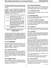
2.0 THE
8051
FAMILY
The
8051
is
a stand-alone high-performance single-chip
computer intended for use
in
sophisticated real-time
applications such as instrumentation, industrial control
and intelligent computer peripherals. It provides the
hardware features, architectural enhancements and new
instructions that make it a powerful and cost effective
controller for applications requiring up to 64K-bytes of
program memory
and/
or
up to 64K-bytes
of
data storage.
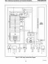
A Block Diagram
is
shown in Figure
3.
The
8031
is
a control-oriented
CPU
without on-chip
program memory.
It
can address 64K-bytes
of
external
Program Memory in addition to 64K-bytes
of
External
Data Memory.
For
systems requiring extra capability,
each member of the
8051
family can
be
expanded using
standard memories
and
the byte oriented MCS-80 and
MCS-85 peripherals. The
8051
is
an
8031
with the lower
4K-bytes
of
Program Memory filled with on-chip mask
programmable
ROM while the
8751
has 4K-bytes
ofUV-
light-erasable/ electrically-programmable ROM.
The three pin-compatible versions
of
this component
reduce development problems to a minimum and provide
maximum flexibility. The
8751
is
well
suited for develop-
2
ment, prototyping, low-volume production
and
applica-
tions requiring field updates; the
8051
for low-cost,
high-volume production and the
8031
for applications
desiring the flexibility
of
external Program Memory
which can be easily modified
and
updated in the field.
2.1
MACRO-VIEW OF THE
8051
ARCHI-
TECTURE
On a single die the
8051
microcomputer combines CPU;
non-volatile 4K x 8 read-only program memory; volatile
128
x 8 read/write data memory;
32
I/O
lines; two 16-bit
timer / event counters; a five-source, two-priority-Ievel,
nested interrupt structure; serial
I/O
port for either multi-
processor communications,
I/O
expansion,
or
full duplex
UART; and on-chip oscillator and clock circuits. This
section will provide an overview
of
the
8051
by providing
a high-level description
of
its major elements: the
CPU
architecture and the on-chip functions peripheral to the
CPU. The generic term "8051"
is
also used to refer collec-
tively to the
8031,
8051,
and
8751.
2.1.1
8051
CPU Architecture
The
8051
CPU
manipulates
operands
in
four
memory
spaces. These are the 64K-byte Program Memory, 64K-
byte External
Data
Memory, 384-byte Internal
Data
Memory and 16-bit Program Counter spaces. The Inter-
nal
Data
Memory address space
is
further divided into the
256-byte Internal
Data
RAM
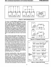
and 128-byte Special
Function Register
(SFR) address spaces shown in Figure
2.1. Four Register Banks (each with eight registers),
128
addressable bits, and the stack reside in the Internal
Data
RAM. The stack depth
is
limited only by the available
Internal Data
RAM
and its location
is
determined by the
8-bit
Stack Pointer.
All
registers except the Program
Counter and the four 8-Register Banks reside in the
Special Function Register address space. These memory
mapped registers include arithmetic registers, pointers,
I/O
ports, and registers for the interrupt system, timers
and serial channel.
128
bit locations in the
SFR
address
space are addressable as bits. The
8051
contains
128
bytes
of Internal Data RAM and
20
SFRs.
The
8051
provides a non-paged Program Memory
address space to accommodate relocatable code.
Con-
ditional branches are performed relative to the Program
Counter. The register-indirect
jump
permits branching
relative to a 16-bit base register with
an
offset provided by
an 8-bit index register. Sixteen-bit jumps and calls permit
branching to any location in the contiguous 64K
Program
Memory address space.
The
8051
has
five
methods for addressing source oper-
ands: Register, Direct, Register-Indirect, Immediate, and
Base-Register- plus Index-Register- Indirect Addressing.
AFN-01488A-06