


8051
Architectural Specification and Functional Description
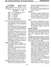
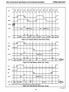
Figure 2.42. The twelve period External
Data
Memory
cycle allows the
80S
1
to
use peripherals that are relatively
slower
than
its program memories. The address
is
emitted
from the processor during T3.
Data
transfer occurs on
the bus during T7 through T12.
TS
and T6
is
the period
during which the direction
of
the bus
is
changed for the.
read operation. The read cycle begins during T2, with the
assertion of address latch enable signal ALE
CD
. The
falling edge of ALE
Q)
is
used
to
latch the address
information, which
is
present on the bus
at
this time
CD
'
into the 8282 latch if a non-multiplexed bus
is
desired.
At
TS, the address
is
removed from the
Port
0 bus
and
the processor's bus drivers go
to
the high-impedance
state
0.
The
data
memor~ad
control signal
RD
CD
'
is
asserted during
T7.
RD
causes the addressed
device to enable its bus drivers to the now-released bus.
At some later time, valid
data
will become available on
the bus
® . When the
80S1
subsequently returns
RD
to
the high level
CD
' the addressed device will then float
its bus drivers, relinquishing the bus again
CD
.
Data
Memory
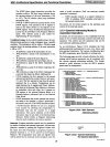
Write Sequence (Figure 2.43)
The write cycle, like the read cycle, begins with the asser-
tion
of
ALE
CD
and
the emission
of
an address
Q)
.
In T6, the processor emits the
data
to be written into the
addressed
data
memory location
CD
. This
data
remains
valid on the bus until the end of the following bus cycle's
T2
0.
The write signal WR goes low
at
T6
CD
and
remains active through
Tl2
® . '
2.11
TIMER/COUNTER
Two independent 16-bit timer/counters are on-board the
80S
1 for use in measuring time intervals, measuring pulse
widths, counting events, and causing periodic (repeti-
tious) interrupts.
2.11.1
Timer/Counter Mode Selection
Counter I can be configured
in
one
of
four modes:
Mode
0)
Provides
an
8-bit counter with a divide-by-32
prescaler
or
an
8-bit timer with a divide-by-32
prescaler. A read/write
ofTHI
accesses counter
l's bits
12-S.
A read/write
of
TLt
accesses
counter
l's bits
7-0.
The programmer should
clear the prescaler (counter I's bits 4-0) before
setting the run flag.
Mode I) Configures counter 1 as a 16-bit timer/counter.
Mode
2)
Configures counter I
as
an 8-bit auto-reload
timer / counter. TH I holds the reload value. TL I
is
incremented. The value
in
TH I
is
reloaded into
TL I when
TLt
overflows from
all
ones (I's). An
8048
compatible counter
is
achieved
by
configur-
ing to mode 2 after zero-ing TH
1.
Mode
3)
When counter I's mode
is
reprogrammed to
mode 3 (from mode
0, I
or
2), it disables the
incrementing
of
the counter. This mode
is
providt;d as an alternative to using the
TR
I
bit
(TCON.6) to start and stop counter I.
28
The serial port receives a pulse each time that counter I
overflows. The standard
U
AR
T modes divide this pulse
rate to generate the transmission rate.
Counter
0 can also
be
configured in one
of
four modes:
Modes
0-2) Modes 0-2 are the same as for counter I.
Mode
3)
In Mode
3,
the configuration
of
THO
is
not
affected by the bits in
TMOD
or
TCON (see
next section).
It
is
configured solely as
an
8-bit
timer that
is
enabled for incrementing by
TCON's
TRI
bit. Upon THO's overflow the
TFI
flag gets set. Thus, neither
TRI
nor
TFI
is
available to counter I when counter 0
is
in
Mode
3.
The function of
TR
I can be done
by
placing counter I in Mode
3,
so only the
function
of
TF
I
is
actually given up by
counter
I.
In Mode
3,
TLO
is configured as
an
8-bit timer/counter and
is
controlled, as usual,
by the Gate
(TMOD.3), CIT (TMOD.2),
TRO
(TCON.4) and
TFO
(TCON.S) control bits.
2.11.2
Configuring the Timer/Counter Input
The use
of
the timer/counters
is
determined by two 8-bit
registers,
TMOD
(timer mode) and TCON (timer
con-"
trol). The counter input circuitry
is
shown
in
Figures
2.46A
and 2.468. The input to the counter circuitry
is
from
an
external reference (for use as a counter),
or
from
the on-chip oscillator (for use as a timer), depending on
whether
TMOD's
CIT bit
is
set
or
cleared, respectively.
When used
as
a time base, the on-chip oscillator
frequency
is
divided
by
twelve (12) before being input to
the counter circuitry. When
TMOD's
Gate bit
is
set (I),
the external reference input (TI,
TO)
or
the oscillator
input
is
gated to the counter conditional upon a second
external input (INTO,
INTI)
being high. When the Gate
bit
is
zero (0), the external reference
or
oscillator input
is
unconditionally enabled. In either case, the normal
interrupt function
of
INTO
and INT I
is
not affected by
the counter's operation. If enabled, an interrupt will
occur when the input at
INTO
or INT I
is
low. The
counters are enabled for incrementing when
TCON's
TR
I and
TRO
bits are set. When the counters overflow
the
TFI
and
TFO
bits
in
TCON get set and interrupt
requests are generated. The functions
of
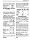
the bits in TCON
are shown in Figure 2.44.
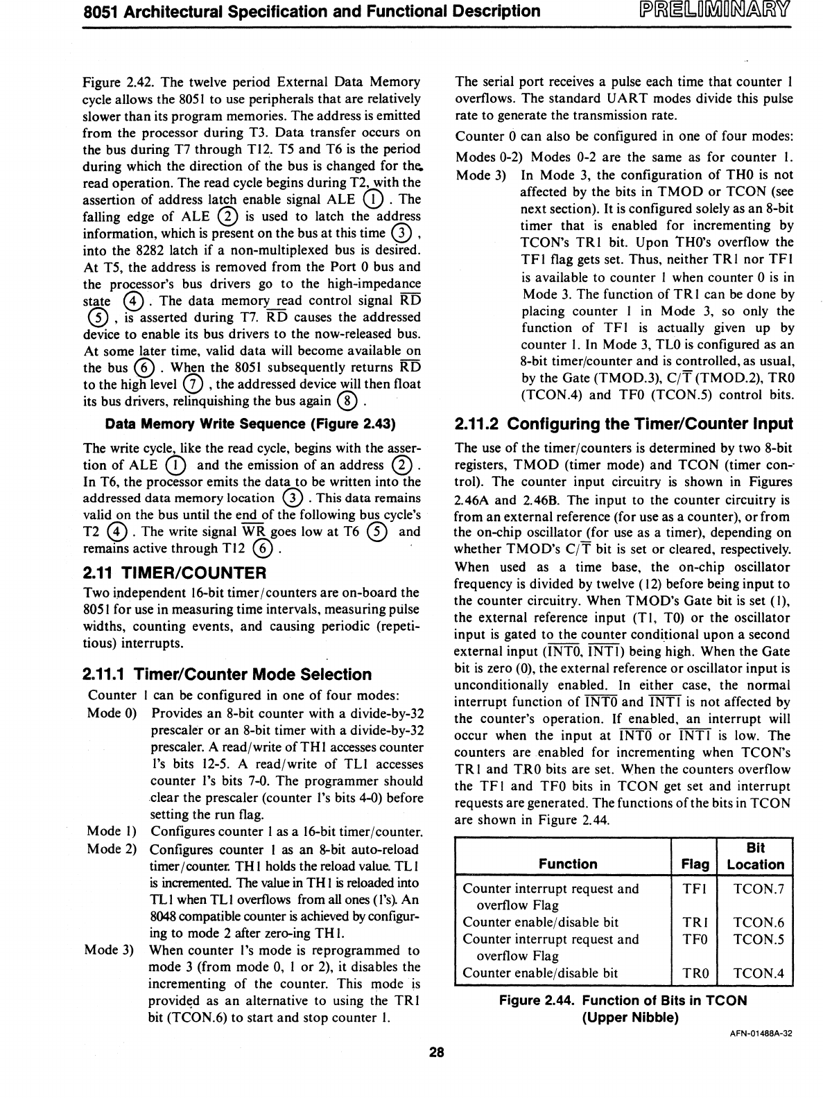
Bit
Function
Flag
Location
Counter interrupt request and
TFI
TCON.7
overflow Flag
Counter enable/disable bit
TRI
TCON.6
Counter interrupt request and
TFO
TCON.S
overflow Flag
Counter enable/disable bit
TRO
TCON.4
Figure 2.44. Function
of
Bits in
TeON
(Upper Nibble)
AFN-01488A-32