


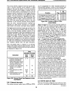


8051
Architectural Specification and Functional Description
last data bit (i.e. ninth or tenth received bit)
is
sampled.
As
long
as
RI
is
set, the loading of SBUF, the updating
of
RB8
and the generation
of
further receiver interrupts
is
inhibited. Thus, overrun
will
occur
if
the programmer
does not reset RI before reception
of
the next frame's last
data bit since the receiver's input shift register will shift in
a third frame.
2.13 EXTERNAL INTERFACE
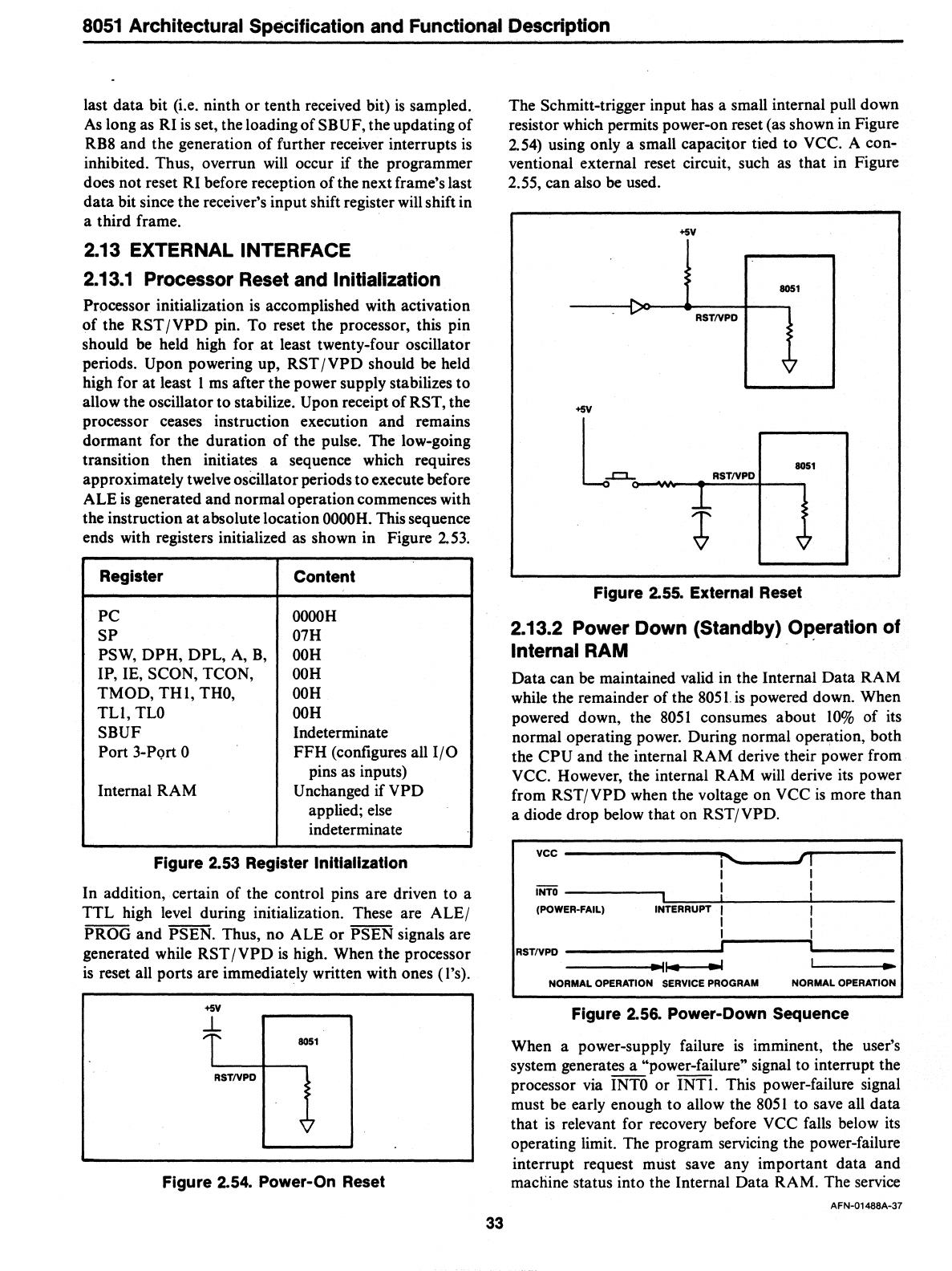
2.13.1 Processor Reset and Initialization
Processor initialization
is
accomplished with activation
of
the RST
/VPO
pin. To reset the processor, this pin
should be held high for
at
least twenty-four oscillator
periods.
Upon powering up, RST
/VPO
should
be
held
high for
at
least I
ms
after the power supply stabilizes
to
allow the oscillator to stabilize. Upon receipt of RST, the
processor ceases instruction execution and remains
dormant for the duration
of
the
pUlse.
The low-going
transition then initiates a sequence which requires
approximately twelve oscillator periods
to
execute before
ALE
is
generated and normal operation commences with
the instruction
at
absolute location
OOOOH.
This sequence
ends with registers initialized as shown in Figure 2.53.
Register
Content
PC
OOOOH
SP
07H
PSW, OPH, OPL,
A,
B,
OOH
IP, IE,
SCaN,
TCON,
OOH
TMOO,
THl,
THO,
OOH
TLl,
TLO
OOH
SBUF
Indeterminate
Port 3-PQrt 0
FFH
(configures all
I/O
pins as inputs)
Internal RAM
Unchanged if
VPO
applied; else
indeterminate
Figure 2.53 Register Initialization
In addition, certain of the control pins are driven to a
TTL high level during initialization. These are ALE/
PROG and PSEN. Thus, no ALE or PSEN signals are
generated while RST /
VPD
is
high. When the processor
is
reset all ports are immediately written with ones (l's).
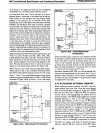
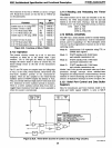
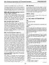
+5V
t
8051
RSTNPD
Figure 2.54. Power-On Reset
33
The Schmitt-trigger input has a small internal pull down
resistor which permits power-on reset (as shown in Figure
2.54) using only a small capacitor tied to
VCe.
A con-
ventional external reset circuit, such as that in Figure
2.55, can also be used.
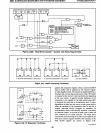
+5V
8051
....
v
RSTNPD
+5V
L
8051
~o-~~-._R_S_TN_P_O;-
____
~
t
Figure 2.55. External Reset
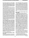
2.13.2 Power Down (Standby) Operation of
Internal RAM
Data can be maintained valid in the Internal Data RAM
while the remainder of the
8051
is
powered down. When
powered down, the
8051
consumes about
10%
of its
normal operating power. During normal operation, both
the
CPU
and the internal RAM derive their power from
VCC. However, the internal RAM
will
derive its power
from
RST/VPD
when the voltage on VCC
is
more than
a diode drop below that on
RST/VPD.
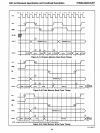
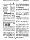
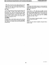
VCC
---------i'-
......
___
rffl----
I I
wro~~--------~~~~~I
__
------+I
____
----
__
I I I
(POWER·FAIL) INTERRUPT I I
I I
I I
~i-----tl
____
__
RSTNPO
--------_.
•
NORMAL OPERATION SERVICE
PROGRAM
NORMAL OPERATION
Figure 2.56. Power-Down Sequence
When a power-supply failure
is
imminent, the user's
system generates a
"power-failure" signal to interrupt the
processor via
INTO
or INTI. This power-failure signal
must be early enough to allow the
8051
to save all data
that
is
relevant for recovery before VCC falls below its
operating limit. The program servicing the power-failure
interrupt request must save any important data and
machine status into the Internal Data RAM. The service
AFN-01488A-37