


8051
Architectural Specification and Functional Description
The 64K-byte External Data Memory address space.is
automatically accessed when the
MOVX instruction
is
executed.
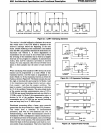
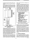
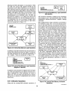
Functionally the Internal Data Memory
is
the most flex-
ible of the address spaces. The Internal Data Memory
space
is
subdivided into a 256-byte Internal Data RAM
address space and a 128-byte
Special Function
Register"'
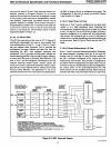
address space as shown in Figure
2.
12.
SPECIAL
FUNCTION
INTERNAL
DATA
RAM REGISTERS
( A ,,------A--,
255
128
55-
ADORE
ABLE
BITS IN
RAM
(128
BIT
S)
REGISTE
RS
-<
48
-
32
24
-
16
8
0
255 255
248
128
135 128
-~
127
127 120
7
0
R7
BANK 3
RO
R7
RD
BANK 2
R7
BANK 1
RO
R7
BANKO
RO
~
F8H
FOH
E8H
EOH
D8H
DOH
C8H
COH
B8H
BOH
A8H
AOH
98H
90H
88H
80H
INTERNAL SPECIAL FUNCTION
DATA
RAM REGISTERS
ADDRESS-
ABLE
BITS IN
SFRs
(128 BITS)
Figure 2.12. Internal Data
Memory
Address Space
The Internal Data
RAM
address space
is
0 to
255.
Four
8-Register Banks occupy locations 0 through
31.
The
stack can
be
located anywhere in the Internal Data RAM
address space. In addition,
128
bit locations of the on-chip
RAM are accessible through Direct Addressing. These
bits reside in Internal Data RAM at byte locations
32
through
47.
Currently locations 0 through
127
of
the
Internal Data RAM address space are filled with on-chip
RAM. Locations
128
through
255
may be filled on later
products without affecting existing software.
The stack depth
is
limited only
by
the available Internal
Data RAM, thanks to an 8-bit reloadable
Stack Pointer.
The stack
is
used for storing the Program Counter during
subroutine calls and may be used for passing parameters.
Any byte of Internal Data RAM or
Special Function
12
Register accessible through Direct Addressing can be
pushed
I popped.
The
Special Function Register address space
is
128
to
255.
All registers except the Program Counter and the four
8-Register Banks reside here. Memory mapping the
Special Function Registers allows them to be accessed as
easily as internal RAM. As such, they can
be
operated on
by most instructions. In addition,
128
bit locations within
the
Special Function Register address space can be
accessed using Direct Addressing. These bits reside in the
Special Function Register byte locations divisible
by
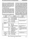
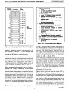
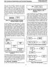
eight. The twenty Special Function Registers are listed
in Figure
2.
13.
Their mapping in the Special Function
Register address space
is
shown in Figure
2.14.
ARITHMETIC
REGISTERS:
ACCumulator*, B register*,
Program Status Word*
POINTERS:
Stack Pointer, Data Pointer (high & low)
PARALLEL I/O PORTS:
Port
3*,
Port
2*,
Port
1*,
Port 0*
INTERRUPT SYSTEM:
Interrupt Priority Control*,
Interrupt Enable Control*
TIMERS:
Timer MODe, Timer CONtrol*, Timer 1
(high & low), Timer 0 (high & low)
SERIAL 1/0 PORT:
Serial
CONtrol*,
Serial data
BUFfer
*Bits
in
these registers are
bit
addressable
Figure 2.13. Special Function Registers
Performing a read from a location of the Internal Data
Memory where neither a byte
of
Internal Data RAM (i.e.
RAM
addresses 128-255) nor a Special Function Register
exists
will
access data of indeterminable value.
Architecturally, each-memory space
is
a linear sequence
of
8-bit wide bytes.
By
Intel convention the storage of
multi-byte address and data operands in program and
data memories
is
least significant byte
at
the low-order
address and the most significant byte
at
the high-order
address. Within byte X, the most significant bit
is
repre-
sented by X.7 while the least significant bit
is
X.O.
Any
deviation from these conventions
will
be explicitly stated
in
the text.
2.4 OPERAND ADDRESSING
There are five methods of addressing source operands.
They
are
Register
Addressing,
Direct
Addressing,
Register-Indirect Addressing, Immediate Addressing,and
Base-Register- plus Index-Register- Indirect Addressing.
The first three of these methods can also
be
used to
AFN-01488A-16