


8051
Architectural Specification and Functional Description
as
an
input
or
an
output and each can be reconfigured
dynamically (i.e., on-the-fly) under software control.
An instruction that
uses
a port's bit/byte
as
a source
operand reads a value that
is
the logical and
of
the last
value written to the bit / byte and the polarity being
applied to the pin/pins by an external device (this
assumes that none
of
the 8051's electrical specs are being
violated). An instruction that reads a bit/byte, operates
on the content, and writes the result back to the bit/byte,
reads the last value written to the bit/byte instead
ofthe
logic level
at
the pin/pins. Pins comprising a single port
can be made a mixed collection of inputs and outputs by,
writing a
"one" to each pin that
is
to be an input. Each
time an instruction uses a port
as
the destination, the
operation must write
"ones" to those bits
that
correspond
to the input pins. An input to a port pin need not
be
synchronized to the oscillator. Each port pin
is
sampled
near the falling-edge
of
ALE during the read instruction's
tenth
or
twenty-second oscillator period. If an input
is
in
transition when it
is
sampled near the falling-edge
of
ALE
it
will
be read as an indeterminate value.
The instructions that perform a read
of,operation on, and
write to a port's bit/byte are INC, DEC, CPL, JBC,
CJNE, DJNZ, ANL,
0 RL, and XRL. The source read by
these operations
is
the last value that was written to the
port, without regard to the levels being applied at the
pins. This insures that bits written to a one
(I)
for use as
inputs are not inadvertently cleared.
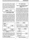
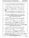
See Figure 2.40.
.
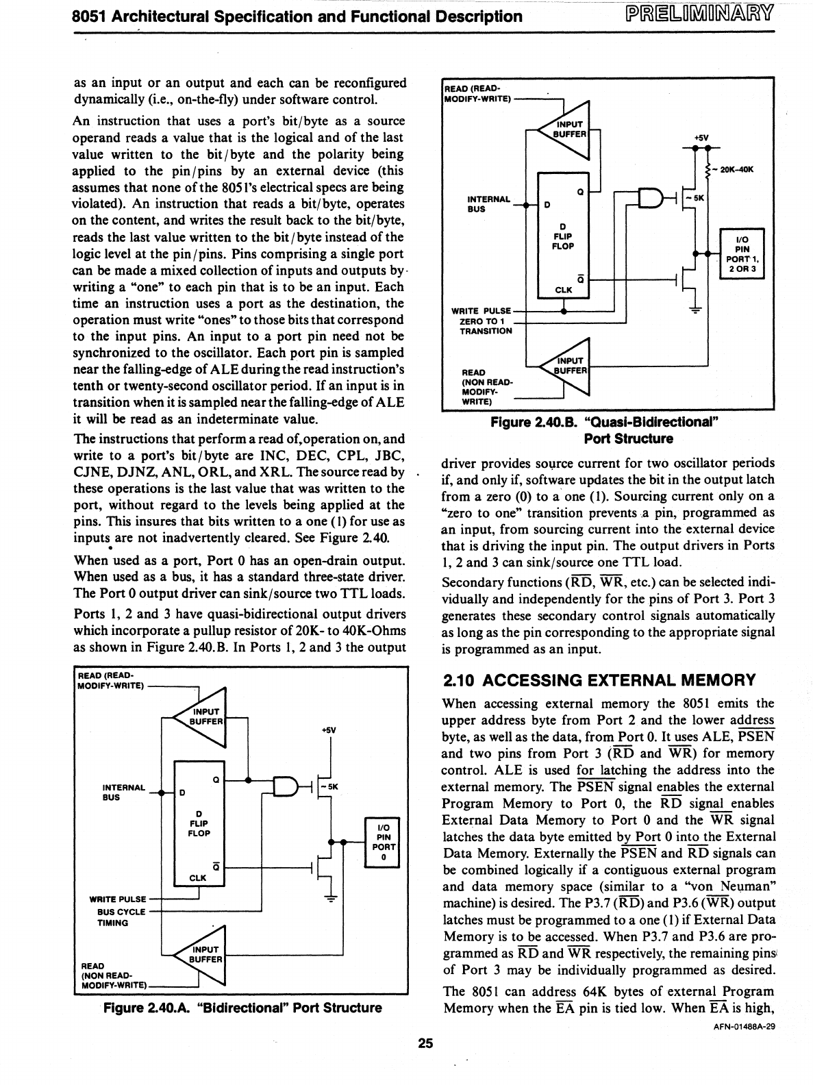
When used as a port, Port 0 has
an
open-drain output.
When used as a bus, it has a standard three-state driver.
The Port
0 output driver can sink/source two
TTL
loads.
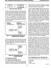
Ports I, 2 and 3 have quasi-bidirectional output drivers
which incorporate a pullup resistor of
20K- to 40K-Ohms
as shown in Figure 2.40.B. In Ports
1,
2 and 3 the output
READ (READ-
MODIFY-WRITE)
-----,
INTERNAL
BUS
WRITE PULSE
BUS
CYCLE
TIMING
READ
(NON READ-
MODIFY-WRITE)
0
0
FLIP
FLOP
CLK
+5V
Q
Q
":"
Figure 2.40.A. "Bidirectional" Port Structure
25
READ (READ-
MODIFY-WRITE)
----,
INTERNAL
BUS
D
o
FLIP
FLOP
CLK
Q
Q
1--+-+----1
WRITE
PULSE-+--..----'
ZERO TO ,
TRANSITION
READ
(NON READ-
MODIFY-
WRITE)
+5V
- 2OK-40K
1/0
PIN
PORT",
20R3
Figure 2.40.B. "Quasi-Bidirectional"
Port
Structure
driver provides
s01,lrce
current for two oscillator periods
if,
and only if, software updates the bit in the output latch
from a zero
(0)
to a one (I). Sourcing current only on a
"zero to one" transition prevents.a pin, programmed as
an
input, from sourcing current into the external device
that
is
driving the input pin. The output drivers in Ports
1,2
and 3 can sink/source one TTL load.
Secondary functions (RD, WR, etc.) can be selected
indi-
vidually and independently for the pins of Port
3.
Port 3
generates these secondary control signals automatically
as long as the pin corresponding to the appropriate signal
is
programmed as
an
input.
2.10
ACCESSING
EXTERNAL
MEMORY
When accessing external memory the
8051
emits the
upper address byte from Port 2 and the lower address
byte, as well as the data, from Port
O.
It uses ALE, PSEN
and two pins from Port 3
(RD
and WR) for memory
control. ALE
is
used for latching the address into the
external memory. The
PSEN signal enables the external
Program Memory to Port
0,
the
RD
signal enables
External Data Memory to Port
0 and the WR signal
latches the data byte emitted by Port
0 into the External
Data Memory. Externally the
PSEN and
RD
signals can
be combined logically if a contiguous external program
and data memory space (similar to a
"von
Ne1,lman"
machine)
is
desired. The P3.7 (RD) and P3.6 (WR) output
latches must
be
programmed to a one
(1)
if External Data
Memory
is
to
be accessed. When P3.7 and P3.6 are pro-
grammed
as
RD and WR respectively, the remaining pins
i
of Port 3 may be individually programmed
as
desired.
The
8051
can address 64K bytes
of
external Program
Memory when the EA pin
is
tied low. When EA
is
high,
AFN-01488A-29