


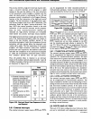


8051 Architectural Specification and Functional Description
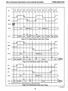
- WR (P3.6). The write control signal latches the data
byte from Port
0 into the External Data Memory.
-RD
(P3.7). The read control signal enables External
Data Memory to
Port
O.
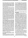
RSTNpD
.
A
low
to high transition on this pin (at approximately
3V)
resets the
80S
1.
If
VPD
is
held within its spec (ap-
proximately
+SV),
while VCC drops below spec, VPD
will provide standby power to the RAM. When VPD
is
low, the RAM's current
is
drawn from VCC. A small
internal resistor permits power-on reset using only a
capacitator connected to VCC.
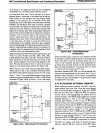
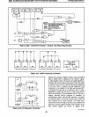
ALE/PROG .
Provides Address Latch Enable output used for latching
the address into external memory during normal opera-
tion. Receives the program pulse input during
EPROM
programming.
36
PSEN
The Program Store Enable output
is
a control signal that
enables the external Program Memory to the bus during
normal fetch operations.
EAlVDD
When held
at
a TTL high level, the
80S
I executes
instructions from the internal
ROM/EPROM
when the
PC
is
less
than 4096. When held
at
a TTL low level, the
80S
I fetches all instructions from external Program
M~mory.
The pin also receives the
21
V EPROM
programming supply voltage.
XTAL 1
Input to the oscillator's high gain amplifier. A crystal or
external source can
be
used.
XTAL 2
Output from the oscillator's amplifier. Required when a
crystal
is
used.
AFN·01488A·40