


8051
Architectural Specification and Functional OescripUon
included in the assembly listing,
or
on
another
file.
The object code generated may
be
used
t.o
program the
8751
EPROM
version
of
the chip or sent
to
Intel for
fabricating the
8051
RO M version. The assembler output
can also
be
debugged using the
ICE-51
in-circuit emulator.
8048 to 8051 Assembly
Langu~ge
Converter
Utility Program
(CONV51)
The
8048
to
8051
assembly language converter
is
a utility
to help users of the
MCS-48 family of microcomputers
upgrade
their
designs
to
the
high
performance
8051
architecture.
By
converting 8048 source code to
8051
source code, the investment
in
software developed for
the
8048
is
maintained when the system
is
upgraded.
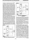
8051 Emulation
BO.ard
(EM-51)
The EM-51
8051
emulation board
is
a small (2.85" x
5.25;
board which emulates an 8031/8051/8751 micro-
computer using standard PROMs
or
EPROMs in place
of
the 8051's on-chip program memory. The board in-
cludes
a
modified
8051
microcomputer,
supporting
circuits, and two sockets for program memory. The user
may select two
2716
EPROMs, a 2732 EPROM,
or
two
3636
J:>ipolar
PROMs depending on crystal frequency
and power requirements.
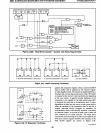
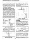
8051 In-Circuit Emulator (ICE-51™)
The
8051
In-Circuit
Emulator
resides in
the
Intellec
development system. The development system interfaces
with the user's
8051
system through an in-cable module
with the cable terminating in an
8051
pin-compatible
plug. Together these replace. the
8051
device
in
the sys-
tem. With the emulator plug in place, the designer can
exercise
the.
system
in
real-time while collecting up to
255
instruction cycles of real-time data. In addition,
he
can
single step the system program.
Static RAM memory
is
available in the ICE-51 module to emulate the 8051's
internal and external program memories and external
data memory. The designer can display and alter the
contents
of
intermil
8051
registers, internal data RAM,
Special Function Registers, and replacement external
memory. Symbolic reference capability allows the
de-
signer to use meaningful symbols provided
by
ASM51
rather than absolute values when examing and modifying
the memory, registers, flags, and
I/O
ports
in
his system.
Universal PROM Programmer Personality
Card (UPP-851)
The UPP-851
is
a personality card for the UPP-\03
Universal PROM Programmer. The Universal PROM
Programmer
is
an Intellec system peripheral capable
of
programming and verifying the
8751.
Programming and
verification
operations
are
initiated from the Intellec
. development system console and are controlled
by
the
Universal
PROM Mapper (UPM) program.
35
8051 Workshop
The workshop provides the design engineer
or
system
designer hands-on experience with the
8051
microcom-
puters. The course includes explanation
of
the Intel
8051
architecture, system timing and input / output design. Lab
sessions
will
allow the attendee to gain detailed familiar-
ity with the
8051
family and support tools.
INSITE™ Library
The
INSITE
Library
contains
8051
utilities
and
applications programs.
2.17
8051
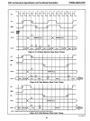
FAMILY PIN DESCRIPTION
VSS
Circuit ground potential.
Vee
+SV
power supply during operation, programming
and
verification.
Port 0
Port
0 is
an
8-bit open drain bidirectional 110 port.
It
is
also the multiplexed low-order address
and
data
bus
when using
~xternal
memory. It
is
used for
data
input
and
output during programming and verification. Port 0 can
sinkl source two
TTL
loads.
Port 1
Port 1
is
an
8-bit quasi-bidirectional
I/O
port.
It
is used
for the low-order address byte during programming
and
verification.
Port
I can sinkl source one
TTL
load.
Port 2
Port
2
is
an
8-bit quasi-bidirectional 110 port.
It
also
emits the high-order 8 bits
of
address when aa:essing
external memory.
It
is
used for the high-order address and
the control signals during programming and verification.
Port
2 can sink/ source one
TTL
load.
Port 3
Port 3
is
an
8-bit quasi-bidirectional 110 port.
It
also
contains the interrupt, timer, serial
port
and
RD
and
WR
pins that are used by various options. The output latch
corresponding to a special function must be programmed
to
a one
(I)
for that function
to
operate. Port 3 can
sink/ source one
TTL
load. The special functions are
assigned to the pins
of
Port 3, as follows:
-
RXD
/ data (P3.0). Serial port's receiver data input
(asynchronous)
or
data input I output (synchronous).
- TXD/clock (P3.I). Serial port's transmitter data
output (asynchronous)
or
clock output (synchronous).
-
INTO
(P3.2). Interrupt 0 input
or
gate control input for
counter
O.
- INTI (P3.3). Interrupt 1 input
or
gate control input for
counter
1.
-
TO
(P3.4). Input to counter O .
-
TI
(P3.5). Input to counter
1.
AFN-Ol488A-39