


8051
Architectural Specification and Functional Description
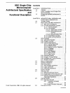
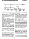
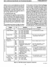
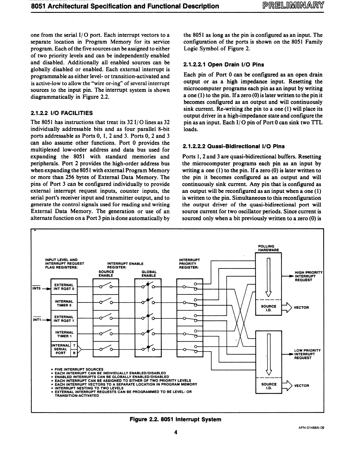
one from the serial
I/O
port. Each interrupt vectors to a
separate location
in
Program Memory for its service
program. Each
of
the
five
sources can
be
assigned to either
of two priority levels and can
be
independently enabled
and disabled. Additionally all enabled sources can
be
globally disabled
or
enabled. Each external interrupt
is
programmable as either level-
or
transition-activated and
is
active-low to allow the "wire or-ing" of several interrupt
sources
.to
the input pin. The interrupt system
is
shown
diagrammatically in Figure 2.2.
2.1.2.2 1/0 FACILITIES
The
8051
has instructions that treat its
32
I/O
lines as
32
individually addressable bits and as four parallel 8-bit
ports addressable as
Ports 0,
1,2
and
3.
Ports
0,2
and 3
can also assume other functions.
Port 0 provides the
multiplexed low-order address and data bus
used,
for
expanding the
8051
with standard memories and
peripherals.
Port 2 provides the high-order address bus
when expanding the
8051
with external Program Memory
or
more than
256
bytes
of
External Data Memory. The
pins of
Port 3 can
be
configured individually to provide
external interrupt request inputs, counter inputs, the
serial port's receiver input and transmitter output, and to
generate the control signals used for reading and writing
External Data Memory. The generation
or
use
of
an
alternate function
on
a Port 3 pin
is
done automatically by
INPUT LEVEL AND
INTERRUPT
REQUEST INTERRUPT ENABLE
FLAG
REGISTERS:
REGISTER:
SOURCE
GLOBAL
ENABLE
ENABLE
eXTERNAL
..AI'"
INTO
......
INTRQST0
INTERNAL
.....
...AI"'"
TIMER 0
I"'"
EXTERNAL
......
INT
RQST 1
-
tNT1
INTERNAL
I'"
TIMER 1
INTERNAL~
r:.
SERIAL
,..
PORT R
• FIVE INTERRUPT SOURCES
•
EACH INTERRUPT CAN BE INDIVIDUALLY ENABLED/DISABLED
•
ENABLED INTERRUPTS CAN BE GLOBALLY ENABLED/DISABLED
the
8051
as
long as the pin is configured as an input. The
configuration
of
the ports is shown
on
the
8051
Family
Logic
Symbol
of
Figure
2.
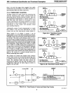
2.1.2.2.1 Open Drain 1/0 Pins
Each pin
of
Port 0 can be configured as
an
open drain
output
or
as a high impedance input. Resetting the
microcomputer programs each pin as
an
input
by
writing
a one (I) to the pin.
Ifa
zero
(0)
is later written to the pin it
becomes configured as
an
output and will continuously
sink current. Re-writing the pin to a one (I) will place its
output driver in a high-impedance state and configure the
pin
as
an
input. Each
I/O
pin
of
Port 0 can sink two TTL
loads.
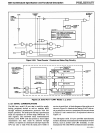
2.1.2.2.2 Quasi-Bidirectional
1/0
Pins
Ports
1,2
and 3 are quasi-bidirectional buffers. Resetting
the microcomputer programs each pin as
an
input by
writing a one
(l)
to the pin. If a zero (0)
is
later written to
the pin it becomes configured as an output and
will
continuously sink current. Any pin that is configured as
an
output will
be
reconfigured as
an
input when a one (I)
is
written to the pin. Simultaneous to this reconfiguration
the output driver
of
the quasi-bidirectional port
will
source current for two oscillator periods. Since current
is
sourced only when a bit previously written to a zero
(0)
is
INTERRUPT
PRIORITY
REGISTER:
-
POLLING
HARDWARE
V
1-----
SOURCE
I.D.
V
-----
------
=>
r--
HIGH PRIORITY
INTERRUPT
REQUEST
VECTOR
LOW PRIORITY
INTERRUPT
REQUEST
•
EACH INTERRUPT CAN BE ASSIGNED TO EITHER OF TWO PRIORITY LEVELS
~
• EACH INTERRUPT VECTORS TO A SEPARATE LOCATION IN PROGRAM MEMORY
SOURCE
•
INTERRUPT NESTING TO TWO LEVELS
I.D.
VECTOR
•
EXTERNAL INTERRUPT REQUESTS CAN BE PROGRAMMED
TO
BE LEVEL-
OR
TRANSITION-ACTIVATED
Figure 2.2. 8051
Interrupt
System
AFN-01488A-08
4