


164
CHAPTER 7 CLOCK GENERATOR
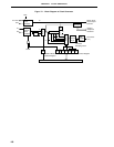
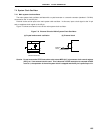
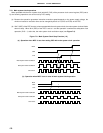
Write to OSMS
(MCS 0)
f
XX
Max. 2/f
X
Operating at f
XX
= f
X
/2 (MCS = 0) Operating at f
XX
= f
X
/2 (MCS = 0)
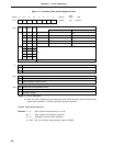
MCS
Main System Clock Scaler Control
0
1
Scaler used
Scaler not used
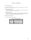
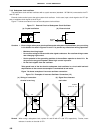
000 0OSMS FFF2H
765432Symbol
1
0 MCS
0
0
Address
After
Reset
R/W
00H W
0
(2) Oscillation mode selection register (OSMS)
This register specifies whether the clock output from the main system clock oscillator without passing through
the scaler is used as the main system clock, or the clock output via the scaler is used as the main system
clock.
OSMS is set with 8-bit memory manipulation instruction.
RESET input sets OSMS to 00H.
Figure 7-4. Oscillation Mode Selection Register Format
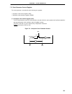
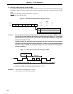
Cautions 1. The main system clock cycle is longer by up to 2/fx only when writing data to OSMS (including
when writing the same data that was written previously) as shown in Figure 7-5. This causes
a temporary error in the count clock cycle of timers in the peripheral hardware that operates
with the main system clock.
In addition, when the oscillation mode is changed, the clocks provided for the peripheral
hardware as well as those for the CPU are switched. Therefore, it is recommended that only
one-time writing to OSMS be performed between the reset release and the peripheral
hardware operation.
Figure 7-5. Main System Clock when Writing to OSMS
2. Setting 1 to MCS should be performed after V
DD ≥ 2.7 V.
Remarks fxx : Main system clock frequency (fx or fx/2)
f
x : Main system clock oscillation frequency