


300
CHAPTER 16 SERIAL INTERFACE CHANNEL 0 (
µ
PD78054 Subseries)
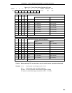
(4) Interrupt timing specify register (SINT)
This register sets the bus release interrupt and address mask functions and displays the SCK0/P27 pin level
status.
SINT is set with a 1-bit or 8-bit memory manipulation instruction.
RESET input sets SINT to 00H.
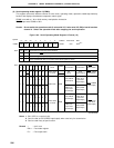
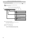
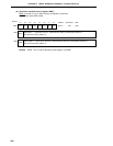
Figure 16-6. Interrupt Timing Specify Register Format
Notes 1. Bit 6 (CLD) is a read-only bit.
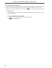
2. When using wake-up function in the SBI mode, set SIC to 0.
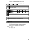
3. When CSIE0 = 0, CLD becomes 0.
Caution Be sure to set bits 0 to 3 to 0.
Remark SVA : Slave address register
CSIIF0 : Interrupt request flag corresponding to INTCSI0
CSIE0 : Bit 7 of serial operating mode register 0 (CSIM0)
<6><5><4>32107
Symbol
SINT 0 CLD SIC SVAM 0 0 0 0
FF63H 00H R/W
Note 1
Address After Reset R/W
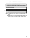
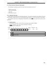
SVAM
0
1
SVA Bit to be Used as Slave Address
Bits 0 to 7
Bits 1 to 7
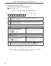
SIC
0
INTCSI0 Interrupt Cause Selection
Note 2
CSIIF0 is set upon termination of serial interface
channel 0 transfer
CSIIF0 is set upon bus release detection or
termination of serial interface channel 0 transfer
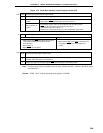
CLD
0
1
SCK0/P27 Pin Level
Note 3
Low level
High level
R/W
R/W
R
1