


193
CHAPTER 8 16-BIT TIMER/EVENT COUNTER
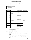
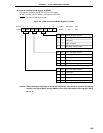
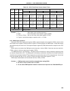
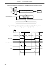
Table 8-6. 16-Bit Timer/Event Counter Interval Times
Minimum Interval Time Maximum Interval Time Resolution
MCS = 1 MCS = 0 MCS = 1 MCS = 0 MCS = 1 MCS = 0
000 2 × TI00 input cycle 2
16
× TI00 input cycle TI00 input edge cycle
0 0 1 Setting 2 × 1/fX Setting 2
16
× 1/fX Setting 1/fX
prohibited (400 ns) prohibited (13.1 ms) prohibited (200 ns)
0102 × 1/fX 2
2
× 1/fX 2
16
× 1/fX 2
17
× 1/fX 1/fX 2
× 1/fX
(400 ns) (800 ns) (13.1 ms) (26.2 ms) (200 ns) (400 ns)
0112
2
× 1/fX 2
3
× 1/fX 2
17
× 1/fX 2
18
× 1/fX 2 × 1/fX 2
2
× 1/fX
(800 ns) (1.6
µ
s) (26.2 ms) (52.4 ms) (400 ns) (800 ns)
1002
3
× 1/fX 2
4
× 1/fX 2
18
× 1/fX 2
19
× 1/fX 2
2
× 1/fX 2
3
× 1/fX
(1.6
µ
s) (3.2
µ
s) (52.4 ms) (104.9 ms) (800 ns) (1.6
µ
s)
1112 × watch timer output cycle 2
16
× watch timer output cycle Watch timer output edge cycle
Other than above Setting prohibited
Remarks 1. fX : Main system clock oscillation frequency
2. MCS : Bit 0 of oscillation mode selection register (OSMS)
3. TCL04 to TCL06 : Bits 4 to 6 of timer clock select register 0 (TCL0)
4. Figures in parentheses apply to operation with f
X = 5.0 MHz
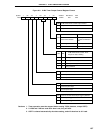
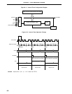
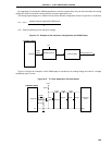
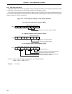
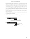
8.5.2 PWM output operations
Setting the 16-bit timer mode control register (TMC0), capture/compare control register 0 (CRC0), and the 16-bit
timer output control register (TOC0) as shown in Figure 8-13 allows operation as PWM output. Pulses with the duty
rate determined by the value set in 16-bit capture/compare register 00 (CR00) beforehand are output from the TO0/
P30 pin.
Set the active level width of the PWM pulse to the high-order 14 bits of CR00. Select the active level with bit 1
(TOC01) of the 16- bit timer output control register (TOC0).
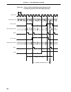
This PWM pulse has a 14-bit resolution. The pulse can be converted to an analog voltage by integrating it with
an external low-pass filter (LPF). The PWM pulse is formed by a combination of the basic cycle determined by 2
8
/
Φ and the sub-cycle determined by 2
14
/Φ so that the time constant of the external LPF can be shortened. Count clock
Φ can be selected with bits 4 to 6 (TCL04 to TCL06) of the timer clock select register 0 (TCL0).
PWM output enable/disable can be selected with bit 0 (TOE0) of TOC0.
Cautions 1. PWM operation mode should be selected before setting CR00.
2. Be sure to write 0 to bits 0 and 1 of CR00.
3. Do not select PWM operation mode for external clock input from the TI00/P00/INTP0 pin.
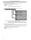
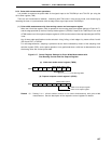
TCL06 TCL05 TCL04