


346
CHAPTER 17 SERIAL INTERFACE CHANNEL 0 (
µ
PD78054Y Subseries)
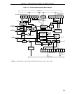
(1) Serial I/O shift register 0 (SIO0)
This is an 8-bit register to carry out parallel-serial conversion and to carry out serial transmission/reception
(shift operation) in synchronization with the serial clock.
SIO0 is set with an 8-bit memory manipulation instruction.
When bit 7 (CSIE0) of serial operating mode register 0 (CSIM0) is 1, writing data to SIO0 starts serial operation.
In transmission, data written to SIO0 is output to the serial output (SO0) or serial data bus (SB0/SB1). In
reception, data is read from the serial input (SI0) or SB0/SB1 to SIO0.
Note that, if a bus is driven in the I
2
C bus mode or 2-wire serial I/O mode, the bus pin must serve for both
input and output. Therefore, the transmission N-ch open-drain output of the device which will start reception
of data must set to high impedance beforehand. Consequently, write FFH to SIO0 in advance.
In the I
2
C bus mode, set SIO0 to FFH with bit 7 (BSYE) of the serial bus interface control register (SBIC) set
to 0.
RESET input makes SIO0 undefined.
Caution Do not execute an instruction that writes SIO0 in the I
2
C bus mode while WUP (bit 5 of the
serial operating mode register 0 (CSIM0)) = 1. Even if such an instruction is not executed,
data can be received when the wake-up function is used (WUP = 1). For the detail of the wake-
up function, refer to 17.4.4 (1) (c) Wake-up function.
(2) Slave address register (SVA)
This is an 8-bit register to set the slave address value for connection of a slave device to the serial bus.
SVA is set with an 8-bit memory manipulation instruction. This register is not used in the 3-wire serial I/O mode.
The master device outputs a slave address for selection of a particular slave device to the connected slave
device. These two data (the slave address output from the master device and the SVA value) are compared
with an address comparator. If they match, the slave device has been selected. In that case, bit 6 (COI) of
serial operating mode register 0 (CSIM0) becomes 1.
Address comparison can also be executed on the data of LSB-masked high-order 7 bits by setting bit 4 (SVAM)
of the interrupt timing specify register (SINT) to (1).
If no matching is detected in address reception, bit 2 (RELD) of the serial bus interface control register (SBIC)
is cleared to 0. In the I
2
C bus mode, the wake-up function can be used by setting the bit 5 (WUP) of CSIM0.
In this case, the interrupt request signal (INTCSI0) is generated when the slave address output by the master
coincides with the value of SVA (the interrupt request signal is also generated when the stop condition is
detected), and it can be learned by this interrupt request that the master requests for communication. To use
the wake-up function, set SIC to 1.
Further, when SVA transmits data as master or slave device in the the I
2
C bus mode or 2-wire serial I/O mode,
errors can be detected using SVA.
RESET input makes SVA undefined.
(3) SO0 latch
This latch holds SI0/SB0/SDA0/P25 and SO0/SB1/SDA1/P26 pin levels. It can be directly controlled by
software.
(4) Serial clock counter
This counter counts the serial clocks to be output and input during transmission/reception and to check whether
8-bit data has been transmitted/received.
(5) Serial clock control circuit
This circuit controls serial clock supply to the serial I/O shift register 0 (SIO0). When the internal system clock
is used, the circuit also controls clock output to the SCK0/SCL/P27 pin.