


357
CHAPTER 17 SERIAL INTERFACE CHANNEL 0 (
µ
PD78054Y Subseries)
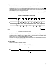
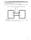
17.4.2 3-wire serial I/O mode operation
The 3-wire serial I/O mode is valid for connection of peripheral I/O units and display controllers which incorporate
a conventional synchronous clocked serial interface as is the case with the 75X/XL, 78K, and 17K series.
Communication is carried out with three lines of serial clock (SCK0), serial output (SO0), and serial input (SI0).
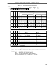
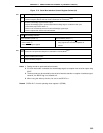
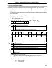
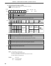
(1) Register setting
The 3-wire serial I/O mode is set with the serial operating mode register 0 (CSIM0) and serial bus interface
control register (SBIC).
(a) Serial operating mode register 0 (CSIM0)
CSIM0 is set with a 1-bit or 8-bit memory manipulation instruction.
RESET input sets CSIM0 to 00H.
Notes 1. Bit 6 (COI) is a read-only bit.
2. Can be used as P25 (CMOS input/output) when used only for transmission.
3. Be sure to set WUP to 0 when the 3-wire serial I/O mode is selected.
Remark × : don’t care
PM×× : Port mode register
P×× : Port output latch
<6><5>43210<7>
Symbol
CSIM0 CSIE0 COI WUP
CSIM04 CSIM03 CSIM02 CSIM01 CSIM00
CSIM01
0
1
Serial Interface Channel 0 Clock Selection
Input Clock to SCK0 pin from off-chip
8-bit timer register 2 (TM2) output
0
2-wire serial I/O mode (See the section 17.4.3, “2-wire serial I/O mode operation”.)
R/W
1 Clock specified with bits 0 to 3 of timer clock select register 3 (TCL3)
CSIM
04
0
CSIM00
×
0
1
FF60H 00H R/W
Note 1
Address After Reset R/W
R/W
CSIM
03
CSIM
02
PM25 P25 PM26 P26
PM27
P27
Operation
Mode
Start Bit
SIO/SB0/SDA0
/P25 Pin Function
SO0/SB1/SDA1
/P26 Pin Function
SCK0/SCL/P27
Pin Function
×
11
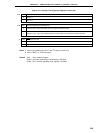
WUP
0
1
Wake-up Function Control
Interrupt request signal generation with each serial transfer in any mode
Interrupt request signal generation when the address received after detecting start condition
(when CMDD = 1) matches the slave address register (SVA) data in I
2
C bus mode
R/W
1
MSB
LSB
1 × 0001
Note 2
3-wire serial
l/O mode
SI0
(Input)
SO0
(CMOS output)
SCK0 (CMOS
input/output)
I
2
C bus mode (See the section 17.4.4, “I
2
C bus mode operation”.)
Note 2
Note 3
Note 2
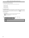
CSIE0
0
Serial Interface Channel 0 Operation Control
Operation stopped
Operation enabled
R/W
1
or