


208
CHAPTER 8 16-BIT TIMER/EVENT COUNTER
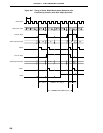
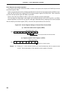
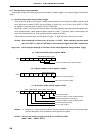
TOC0 110/10/11100
TOE0TOC01LVR0OSPT OSPE TOC04 LVS0
TO0 Output Enabled
Inversion of output on match of TM0 and CR00
Specified TO0 output F/F initial value
Inversion of output on match of TM0 and CR01
One-shot pulse output mode
Set 1 in case of output
CRC0 00/1000000
CRC00CRC01CRC02
CR00 set as compare register
CR01 set as compare register
TMC0 00110000
OVF0TMC01TMC02TMC03
Clear & start with match of TM0 and CR00
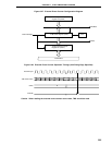
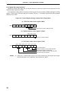
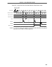
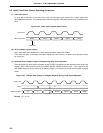
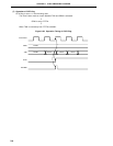
8.5.7 One-shot pulse output operation
It is possible to output one-shot pulses synchronized with a software trigger or an external trigger (TI00/P00 pin
input).
(1) One-shot pulse output using software trigger
If the 16-bit timer mode control register (TMC0), capture/compare control register 0 (CRC0), and the 16-bit
timer output control register (TOC0) are set as shown in Figure 8-31, and 1 is set in bit 6 (OSPT) of TOC0
by software, a one-shot pulse is output from the TO0/P30 pin.
By setting 1 in OSPT, the 16-bit timer/event counter is cleared and started, and output is activated by the count
value set beforehand in 16-bit capture/compare register 01 (CR01). Thereafter, output is inactivated by the
count value set beforehand in 16-bit capture/compare register 00 (CR00).
TM0 continues to operate after one-shot pulse is output. To stop TM0, 00H must be set to TMC0.
Caution When outputting one-shot pulse, do not set 1 in OSPT. When outputting one-shot pulse
again, set OSPT to 1 after the INTTM00, or interrupt match signal with CR00, is generated.
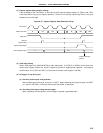
Figure 8-31. Control Register Settings for One-Shot Pulse Output Operation Using Software Trigger
(a) 16-bit timer mode control register (TMC0)
(b) Capture/compare control register 0 (CRC0)
(c) 16-bit timer output control register (TOC0)
Remark 0/1: Setting 0 or 1 allows another function to be used simultaneously with one-shot pulse output.
See the description of the respective control registers for details.
Caution Values in the following range should be set in CR00 and CR01.
0000H
≤ CR01 < CR00 ≤ FFFFH