


59
Input
Input/
output
CHAPTER 3 PIN FUNCTION (
µ
PD78054 Subseries)
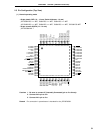
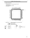
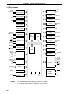
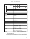
3.1 Pin Function List
3.1.1 Normal operating mode pins
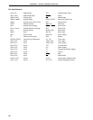
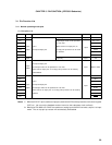
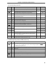
(1) Port pins (1/3)
Pin Name
Input/Output
Function After Reset
Alternate Function
P00 Input Input only Input INTP0/TI00
P01 Input/output mode can be specified INTP1/TI01
P02 in 1-bit units. INTP2
P03 Input/ Port 0. When used as an input port, an INTP3
P04 output 8-bit input/output port. on-chip pull-up resistor can be used INTP4
P05 by software. INTP5
P06 INTP6
P07
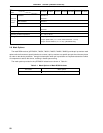
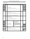
Note1
Input Input only Input XT1
P10 to P17 Port 1.
8-bit input/output port.
Input/output mode can be specified in 1-bit units. Input ANI0 to ANI7
When used as input port, an on-chip pull-up resistor can be used by
software
Note2
.
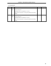
P20 SI1
P21 SO1
P22 Port 2. SCK1
P23 Input/ 8-bit input/output port. STB
P24 output Input/output mode can be specified in 1-bit units. BUSY
P25 When used as an input port, an on-chip pull-up resistor can be used by SI0/SB0
P26 software. SO0/SB1
P27 SCK0
Notes 1. When the P07/XT1 pin is used as an input port, set the bit 6 (FRC) of the processor clock control register
(PCC) to 1 (do not use the feedback resistor internal to the subsystem clock oscillator).
2. When pins P10/ANI0 to P17/ANI7 are used as an analog input of the A/D converter, set port 1 to input
mode. The on-chip pull-up resistor will automatically be disabled.
Input