


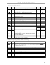
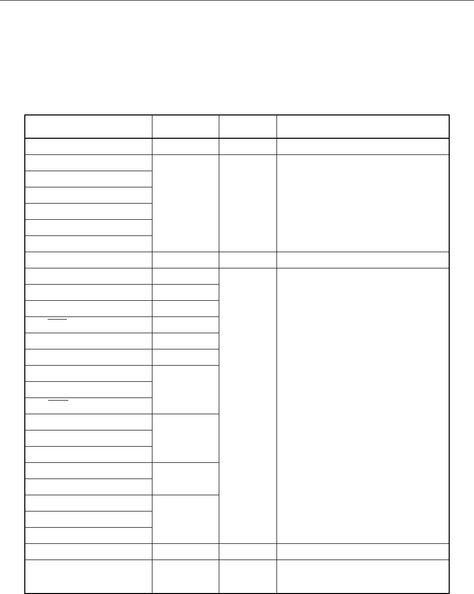
87
CHAPTER 4 PIN FUNCTION (
µ
PD78054Y Subseries)
Input/Output
Circuit Type
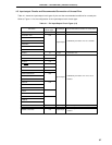
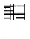
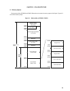
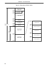
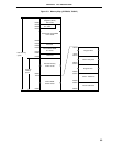
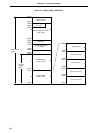
P00/INTP0/TI00 2 Input Connect to VSS.
P01/INTP1/TI01 8-A
P02/INTP2
P03/INTP3 Individually connect to VSS via a resistor.
P04/INTP4
P05/INTP5
P06/INTP6
P07/XT1 16 Input Connect to VDD.
P10/ANI0 to P17/ANI7 11
P20/SI1 8-A
P21/SO1 5-A
P22/SCK1 8-A
P23/STB 5-A
P24/BUSY 8-A
P25/SI0/SB0/SDA0 10-A
P26/SO0/SB1/SDA1 Individually connect to VDD or VSS via a
P27/SCK0/SCL resistor.
P30/TO0 5-A
P31/TO1
P32/TO2
P33/TI1
P34/TI2
P35/PCL 5-A
P36/BUZ
P37
P50/A8 to P57/A15 5-A Input/output
Individually connect to VDD or VSS via a
resistor.
P40/AD0 to P47/AD7 5-E Input/Output Individually connect to VDD via a resistor.
Input/Output
Input/Output
Pin Name Input/Output Recommended Connection of Unused Pins
8-A
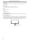
4.3 Input/output Circuits and Recommended Connection of Unused Pins
Table 4-1 shows the input/output circuit types of pins and the recommended conditions for unused pins.
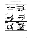
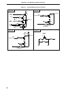
Refer to Figure 4-1 for the configuration of the input/output circuit of each type.
Table 4-1. Pin Input/Output Circuit Types (1/2)