


494
CHAPTER 21 INTERRUPT AND TEST FUNCTIONS
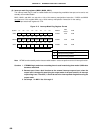
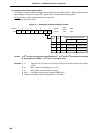
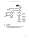
Address
FF47H 00H
After
Reset
R/W
R/W
0
0
1
1
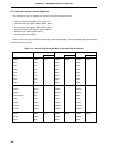
INTP0 Sampling Clock Selection
f
xx
/2
N
f
xx
/2
7
f
xx
/2
5
f
xx
/2
6
SCS1
7
0
Symbol
SCS
6
0
5
0
4
0
3
0
2
0
1
SCS1
0
SCS0
0
1
0
1
SCS0
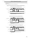
MCS = 1 MCS = 0
f
x
/2
7
(39.1 kHz)
f
x
/2
5
(156.3 kHz)
f
x
/2
6
(78.1 kHz)
f
x
/2
8
(19.5 kHz)
f
x
/2
6
(78.1 kHz)
f
x
/2
7
(39.1 kHz)
Caution fXX/2
N
is a clock to be supplied to the CPU and fXX/2
5
, fXX/2
6
and fXX/2
7
are clocks to be supplied
to the peripheral hardware. fXX/2
N
stops in the HALT mode.
Remarks 1. N : Value (N=0 to 4) at bits 0 to 2 (PCC0 to PCC2) of processor clock control register
(PCC)
2. f
XX : Main system clock frequency (fX or fX/2)
3. fX : Main system clock oscillation frequency
4. MCS : Oscillation mode selection register (OSMS) bit 0
5. Values in parentheses when operated with f
X = 5.0 MHz.
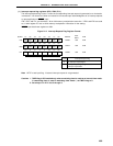
(5) Sampling clock select register (SCS)
This register is used to set the valid edge clock sampling clock to be input to INTP0. When remote controlled
data reception is carried out using INTP0, digital noise is removed with sampling clocks.
SCS is set with an 8-bit memory manipulation instruction.
RESET input sets SCS to 00H.
Figure 21-7. Sampling Clock Select Register Format