


Chapter 3 Hardware
20 Reference Manual XTX 820
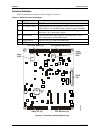
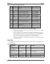
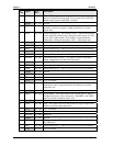
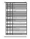
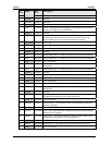
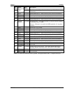
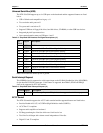
J1
Pin #
Signal PCI
Pin #
Description
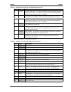
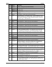
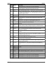
GNT* 17 (A17)
Grant – This is a point-to-point signal and indicates to the agent that
access to the bus has been granted. Every master has its own GNT,
which must be ignored while RST is asserted.
Ground 18 (A18) Ground
57 PME* 19 (A19) Power Management Event – This signal is an optional signal that can
be used by a device to request a change in the device or system
power state.
91 AD30 20 (A20) Address/Data bus 30 – These signals (AD31 – AD0) are multiplexed
on the same PCI connector pins. During the address phase of a PCI
cycle, AD31–AD0 contain a 32-bit address or other destination
information. During the data phase, AD31 – AD0 contain data.
+3.3V 21 (A21) +3.3 Volt Power
87 AD28 22 (A22) Address/Data bus 28 – Refer to Pin-20 (A20) for more information
86 AD26 23 (A23) Address/Data bus 26 – Refer to Pin-20 (A20) for more information
Ground 24 (A24) Ground
81 AD24 25 (A25) Address/Data bus 24 – Refer to Pin-20 (A20) for more information)
60 DEVSEL 26 (A26) Initialization Device Select – This signal is used as a chip select
during configuration read and write transactions.
+3.3V 27 (A27) +3.3 Volt Power
77 AD22 28 (A28) Address/Data bus 22 – Refer to Pin-20 (A20) for more information
75 AD20 29 (A29) Address/Data bus 20 – Refer to Pin-20 (A20) for more information
Ground 30 (A30) Ground
74 AD18 31 (A31) Address/Data bus 18 – Refer to Pin-20 (A20) for more information
69 AD16 32 (A32) Address/Data bus 16 – Refer to Pin-20 (A20) for more information
+3.3V 33 (A33) +3.3 Volt Power
65 FRAME* 34 (A34)
PCI bus Frame access – This signal is driven by the current master to
indicate the start of a transaction and will remain active until the
final data cycle.
Ground 35 (A35) Ground
61 TRDY* 36 (A36) Target Ready – This signal indicates the selected device’s ability to
complete the current cycle of transaction. Both IRDY* and TRDY*
must be asserted to terminate a data cycle.
Ground 37 (A37) Ground
64 STOP* 38 (A38)
Stop – This signal is driven by the current PCI target to request the
master to stop the current transaction.
+3.3V 39 (A39) +3.3 Volt Power
Reserved* 40 (A40) Reserved
Reserved* 41 (A41) Reserved
Ground 42 (A42) Ground
53 PAR 43 (A43)
PCI bus Parity bit – This signal is the even parity bit on AD[31:0]
and CBE[3:0]*.
47 AD15 44 (A44) Address/Data bus 15 – Refer to Pin-20 (A20) for more information
+3.3V 45 (A45) +3.3 Volt Power