


Contents
XTX 820 Reference Manual v
Figure 2-6. XTX 820 Dimensions (Top, Through Board View) ....................................................... 13
Figure 4-1. BIOS Main Setup Screen.............................................................................................. 63
Figure 4-2. BIOS Advanced Setup Screen ..................................................................................... 64
Figure 4-3. BIOS Boot Setup Screen.............................................................................................. 81
Figure 4-4. BIOS Security Setup Screen ........................................................................................84
Figure 4-5. BIOS Power Setup Screen ...........................................................................................86
Figure 4-6. BIOS Exit Setup Screen ...............................................................................................88
List of Tables
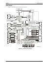
Table 2-1. Major Integrated Circuit Description and Function ........................................................ 11
Table 2-2. Board Connector Descriptions.......................................................................................12
Table 2-3. Weight and Footprint Dimensions.................................................................................. 13
Table 2-4. Power Supply Requirements ......................................................................................... 14
Table 2-5. Environmental Requirements ........................................................................................ 14
Table 3-1. Interrupt Channel Assignments (IRQs)..........................................................................17
Table 3-2. Memory Map .................................................................................................................. 17
Table 3-3. I/O Address Map ............................................................................................................ 18
Table 3-4. Simplified PCI Pin/Signal Descriptions (J1)................................................................... 19
Table 3-5. Simplified USB Interface Pin/Signal Descriptions (J1) .................................................. 24
Table 3-6. Simplified Serial Interrupt Request (J1)......................................................................... 24
Table 3-7. Simplified Audio Interface Pin/Signal Descriptions (J1)................................................. 25
Table 3-8. Complete J1 Interface Pin/Signal Descriptions (J1) ...................................................... 25
Table 3-9. PCI Express Interface Pin/Signal Descriptions (J2) ...................................................... 29
Table 3-10. Serial ATA Interface Pin/Signal Descriptions (J2) ....................................................... 30
Table 3-11. USB 4 & 5 Interface Pin/Signal Descriptions (J2)........................................................ 30
Table 3-12. Audio CODEC Interface Pin/Signal Descriptions (J2) ................................................. 31
Table 3-13. LPC Interface Pin/Signal Descriptions (J2).................................................................. 31
Table 3-14. Miscellaneous Interface Pin/Signal Descriptions (J2).................................................. 32
Table 3-15. Complete J2 Interface Pin/Signal Descriptions (J2) .................................................... 32
Table 3-16. Simplified Floppy Drive Interface Pin/Signal Descriptions (J3).................................... 35
Table 3-17. Simplified Parallel Interface (SPP) Pin/Signal Descriptions (J3) ................................. 36
Table 3-18. Simplified Serial Interface Pin/Signal Descriptions (J3)............................................... 37
Table 3-19. Simplified Keyboard, Mouse, and Infrared (IrDA) Port Pin/Signal Descriptions (J3)... 39
Table 3-20. Simplified CRT Interface Pin/Signal Descriptions (J3) ................................................40
Table 3-21. Simplified LVDS Interface Pin/Signal Descriptions (J3) ..............................................41
Table 3-22. Simplified TV Out (S-Video) Interface Pin/Signal Descriptions (J3) ............................ 42
Table 3-23. Complete J3 Interface Pin/Signal Descriptions (J3) .................................................... 42
Table 3-24. Simplified Primary IDE Interface Pin/Signal Descriptions (J4) .................................... 46
Table 3-25. Simplified Ethernet Port Pin/Signal Descriptions (J4).................................................. 48
Table 3-26. Simplified Power Control and Miscellaneous Pin/Signal Descriptions (J4)................. 50
Table 3-27. SMBus Reserved Addresses....................................................................................... 51
Table 3-28. Complete J4 Interface Pin/Signal Descriptions (J4) .................................................... 51
Table 3-29. SDVO Interface Pin/Signal Descriptions (J6) .............................................................. 55
Table 3-30. Typical ATX Power Interface Pin/Signal Descriptions................................................. 58
Table 3-31. Wake Up Activities and Conditions..............................................................................60
Table 4-1. BIOS Setup Utility Menus ..............................................................................................62
Table 4-2. Exiting and Loading Default Keys..................................................................................63
Table 4-3. Local Flat Panel Type List.............................................................................................. 66