


Chapter 3 Hardware
XTX 820 Reference Manual 23
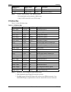
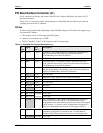
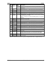
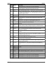
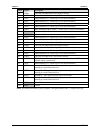
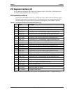
J1
Pin #
Signal PCI
Pin #
Description
49 CBE1* 106 (B44)
Bus Command and Byte Enable 1 – Refer to pin-52 (A52) for more
information.
45 AD14 107 (B45) Address/Data bus 14 – Refer to Pin-20 (A20) for more information
GND 108 (B46) Ground
41 AD12 109 (B47) Address/Data bus 12 – Refer to Pin-20 (A20) for more information
37 AD10 110 (B48) Address/Data bus 10 – Refer to Pin-20 (A20) for more information
NC
66 MHz/
Ground
111 (B49)
66 MHz Enable – This signal indicates to a device if the bus segment
is operating at 66 or 33 MHz.
Ground – If this pin is not used for 66 MHz operation, it is at ground
potential.
GND 112 (B50) Ground for +3.3V boards
GND 113 (B51) Ground for +3.3V boards
33 AD08 114 (B52) Address/Data bus 08 – Refer to Pin-20 (A20) for more information
32 AD07 115 (B53) Address/Data bus 07 – Refer to Pin-20 (A20) for more information
+3.3V 116 (B54) +3.3 Volt Power
30 AD05 117 (B55) Address/Data bus 05 – Refer to Pin-20 (A20) for more information
28 AD03 118 (B56) Address/Data bus 03 – Refer to Pin-20 (A20) for more information
Ground 119 (B57) Ground
25 AD01 120 (B58) Address/Data bus 01 – Refer to Pin-20 (A20) for more information
+3.3V(I/O) 121 (B59) +3.3V I/O
NC ACK64* 122 (B60) Acknowledge 64-bit Transfer – This signal indicates the target is
willing to transfer data using 64 bits. Not used in 32-bit system.
NC +5V 123 (B61) +5 Volt Power
NC +5V 124 (B62) +5 Volt Power
Notes: The shaded area denotes power or ground. The signals marked with * = Negative true logic.