


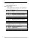

Chapter 3 Hardware
22 Reference Manual XTX 820
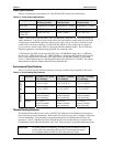
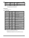
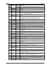
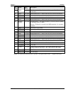
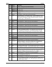
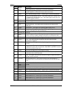
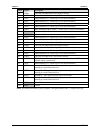
J1
Pin #
Signal PCI
Pin #
Description
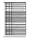
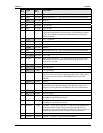
Ground 74 (B12) Ground
Ground 75 (B13) Ground
Reserved 76 (B14) Reserved
Ground 77 (B15) Ground
CLK 78 (B16) Clock – This signal provides timing for all transactions on the PCI
bus and is an input to every PCI device.
Ground 79 (B17) Ground
REQ* 80 (B18) Request – This is a point-to-point signal and indicates to the arbiter
that this agent desires use of the bus. Every master has its own
Request which must be tri-stated while Reset is asserted.
+3.3V(I/O) 81 (B19) +3.3V I/O
94 AD31 82 (B20) Address/Data bus 31 – Refer to Pin-20 (A20) for more information
90 AD29 83 (B21) Address/Data bus 29 – Refer to Pin-20 (A20) for more information
Ground 84 (B22) Ground
89 AD27 85 (B23) Address/Data bus 27 – Refer to Pin-20 (A20) for more information
85 AD25 86 (B24) Address/Data bus 25 – Refer to Pin-20 (A20) for more information
+3.3V 87 (B25) +3.3 Volt Power
82 CBE3* 88 (B26) Bus Command and Byte Enable 3 – Refer to Pin-52 (A52) for more
information.
79 AD23 89 (B27) Address/Data bus 23 – Refer to Pin-20 (A20) for more information
Ground 90 (B28) Ground
78 AD21 91 (B29) Address/Data bus 21 – Refer to Pin-20 (A20) for more information
73 AD19 92 (B30) Address/Data bus 19 – Refer to Pin-20 (A20) for more information
+3.3V 93 (B31) +3.3 Volt Power
71 AD17 94 (B32) Address/Data bus 17 – Refer to Pin-20 (A20) for more information
70 CBE2* 95 (B33) Bus Command and Byte Enable 2 – Refer to Pin-52 (A52) for more
information.
Ground 96 (B34) Ground
63 IRDY* 97 (B35) Initiator Ready – This signal indicates the master’s ability to
complete the current data cycle of the transaction.
+3.3V 98 (B36) +3.3 Volt Power
60 DEVSEL* 99 (B37) Device Select – This signal is driven by the target device when its
address is decoded.
Ground 100 (B38) Ground
59 LOCK* 101 (B39) Lock – This signal indicates an operation that may require multiple
transactions to complete.
55 PERR* 102 (B40)
Parity Error – This signal is driven by the PCI target during a write
to indicate a data parity error has been detected.
+3.3V 103 (B41) +3.3 Volt Power
54 SERR* 104 (B42) System Error – This signal is for reporting address parity errors.
+3.3V 105 (B43) +3.3 Volt Power