


Chapter 3 Hardware
XTX 820 Reference Manual 27
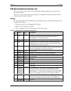
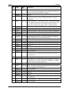
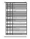
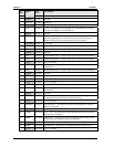
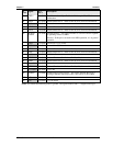
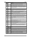
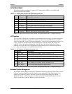
Pin # Signal Description
47 AD15 Address/Data bus 15 – Refer to pin-23 for more information.
48 ASGND
Analog Ground – This ground is used for the sound controller and an
external amplifier to achieved the lowest audio noise levels.
49 CBE1* Bus Command and Byte Enable 1 – Refer to pin-31 for more information.
50 AOUT_R
Stereo Line Output Right channel – This output signal has a nominal level of
1 volt RMS into 10k impedance load. This output signal can not drive low-
impedance speakers directly
51 VCC2 +5 volts +/-%5
52 VCC3 +5 volts +/-%5
53 PAR
PCI bus Parity bit – This signal is the even parity bit on AD[31:0] and
CBE[3:0]*.
54 SERR* System Error – This signal is for reporting address parity errors.
55 PERR*
Parity Error – This signal is driven by the PCI target during a write to
indicate a data parity error has been detected.
56 RESERVED Reserved
57 PME*
Power Management Event – This signal is an optional signal that can be
used by a device to request a change in the device or system power state.
58 USB2- Universal Serial Bus Port 2 Data Negative Polarity
59 LOCK*
Lock – This signal indicates an operation that may require multiple
transactions to complete.
60 DEVSEL* Device Select – This signal is driven by the target device when its address is
decoded.
61 TRDY* Target Ready – This signal indicates the selected device’s ability to
complete the current cycle of transaction. Both IRDY* and TRDY* must be
asserted to terminate a data cycle.
62 USB3- Universal Serial Bus Port 3 Data Negative Polarity
63 IRDY* Initiator Ready – This signal indicates the master’s ability to complete the
current data cycle of the transaction.
64 STOP* Stop – This signal is driven by the current PCI target to request the master to
stop the current transaction.
65 FRAME* PCI bus Frame access – This signal is driven by the current master to
indicate the start of a transaction and will remain active until the final data
cycle.
66 USB2+ Universal Serial Bus Port 2 Data Positive Polarity
67 GND Ground
68 GND Ground
69 AD16 Address/Data bus 16 – Refer to pin-23 for more information.
70 CBE2* Bus Command and Byte Enable 2 – Refer to pin-31 for more information.
71 AD17 Address/Data bus 17 – Refer to pin-23 for more information.
72 USB3+ Universal Serial Bus Port 3 Data Positive Polarity
73 AD19 Address/Data bus 19 – Refer to pin-23 for more information.
74 AD18 Address/Data bus 18 – Refer to pin-23 for more information.
75 AD20 Address/Data bus 20 – Refer to pin-23 for more information.