


Chapter 3 Hardware
28 Reference Manual XTX 820
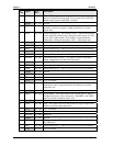
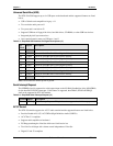
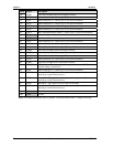
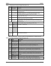
Pin # Signal Description
76 USB0- Universal Serial Bus Port 0 Data Negative Polarity
77 AD22 Address/Data bus 22 – Refer to pin-23 for more information.
78 AD21 Address/Data bus 21 – Refer to pin-23 for more information.
79 AD23 Address/Data bus 23 – Refer to pin-23 for more information.
80 USB1- Universal Serial Bus Port 0 Data Negative Polarity
81 AD24 Address/Data bus 24 – Refer to pin-23 for more information.
82 CBE3* Bus Command and Byte Enable 3 – Refer to pin-31 for more information.
83 VCC4 +5 volts +/-%5
84 VCC5 +5 volts +/-%5
85 AD25 Address/Data bus 25 – Refer to pin-23 for more information.
86 AD26 Address/Data bus 26 – Refer to pin-23 for more information.
87 AD28 Address/Data bus 28 – Refer to pin-23 for more information.
88 USB0+ Universal Serial Bus Port 0 Data Positive Polarity
89 AD27 Address/Data bus 27 – Refer to pin-23 for more information.
90 AD29 Address/Data bus 29 – Refer to pin-23 for more information.
91 AD30 Address/Data bus 30 – Refer to pin-23 for more information.
92 USB1+ Universal Serial Bus Port 1 Data Positive Polarity
93 PCIRST* PCI Bus Reset – This output signal is used to reset the entire PCI Bus and is
asserted during a system reset.
94 AD31 Address/Data bus 31 – Refer to pin-23 for more information.
95 INTC* Interrupt C – This signal is used to request an interrupt and only has
meaning on a multi-function device.
96 INTD* Interrupt D – This signal is used to request an interrupt and only has
meaning on a multi-function device.
97 INTA* Interrupt A – This signal is used to request an interrupt.
98 INTB* Interrupt B – This signal is used to request an interrupt and only has
meaning on a multi-function device.
99 GND Ground
100 GND Ground
Notes: The shaded area denotes power or ground. The signals marked with * = Negative true logic.