User’s Manual
IBM PowerPC 750GX and 750GL RISC Microprocessor
PowerPC 750GX Overview
Page 34 of 377
gx_01.fm.(1.2)
March 27,2006
written into an 8-word buffer. Subsequent double words are fetched from either the L2 cache or the system
memory and written into the buffer. Once the total block is in the buffer, the line is written into the L1 cache in
a single cycle. This minimizes write cycles into the L1 cache, leaving more read/write cycles available to the
LSU. The L1 is nonblocking and supports hits under misses during this block reload sequence. Misaligned
accesses across a block or page boundary can incur a performance penalty. The 750GX L1 data cache
supports miss-under-miss access, meaning that with one miss outstanding, the cache can continue to be
accessed for up to three more misses. The 750GX L1 data cache also allows the additional misses to initiate
a transaction in the bus interface unit, while the first miss is pending.
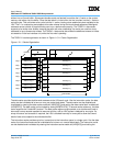
The 750GX L1 cache organization is shown in Figure 1-2, L1 Cache Organization.
The data cache provides double-word accesses to the LSU each cycle. Like the instruction cache, the data
cache can be invalidated all at once or on a per-cache-block basis. The data cache can be disabled and
invalidated by clearing the data-cache enable bit (HID0[DCE]) and setting the data-cache flash invalidate bit
(HID0[DCFI]). The data cache can be locked by setting HID0[DLOCK]. To ensure cache coherency, the data
cache supports the 3-state MEI protocol. The data-cache tags are single-ported, so a simultaneous load or
store and a snoop access represent a resource collision, and an LSU access is delayed for one cycle. If a
snoop hit occurs and a castout is required, the LSU is blocked internally for one cycle to allow the 8-word
block of data to be copied to the write-back buffer.
The instruction cache provides up to four instructions to the instruction queue in a single cycle. Like the data
cache, the instruction cache can be invalidated all at once or on a cache-block basis. The instruction cache
can be disabled and invalidated by clearing the instruction-cache enable bit (HID0[ICE]) and setting the
Figure 1-2. L1 Cache Organization
8 Words/Way
128 Sets
Way 5
Way 6
Way 7
Way 4
Address Tag 4
Address Tag 5
Address Tag 6
Address Tag 7
Way 1
Way 2
Way 3
Way 0
Address Tag 0
Address Tag 1
Address Tag 2
Address Tag 3
State
State
State
Words [0–7]
State
Words [0–7]
Words [0–7]
Words [0–7]
State
State
State
Words [0–7]
State
Words [0–7]
Words [0–7]
Words [0–7]


